This thread has been locked.

If you have a related question, please click the "Ask a related question" button in the top right corner. The newly created question will be automatically linked to this question.

AFE7900EVM: The TX output level is lower than the description in datasheet

Part Number: AFE7900EVM
Other Parts Discussed in Thread: AFE7901, AFE7900

Hi,

According to the datasheet, the AFE7901 TX output is 5.7 dBm for full scale diginal input.

However when we measured our own design, there were several dB missing.

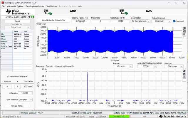
The AFE7900 EVM also shows the same result. With the digital signal of scale factor 1 generated in High Speed Data pro, the level of TXB output signal at around 500 MHz is only 1 dBm.

Could you please advise?

Best regards

Yinan Zhang

  • Hi Yinan,

    We will work on setting this up on our bench in the lab.

    We suspect the missing power might be due to losses on the matching network and balun.

    Best,

    Camilo

  • Hi Camilo,

    How about your measurement?

    Thank you.

    Best
    Yinan

  • Hi Yinan,

    As we spoke today during the meeting, we will work on prioritizing this.

    I will have an update tomorrow on this measurement.

    Best,

    Camilo

  • Hi Yinan,

    I have been able to try this on our bench and I am able to get very close to the datasheet numbers. I created the "S3_6sgps_J56orJ57.py" script below with parameters similar to the ones in the datasheet and sent a -0.1dBFS tone (Scaling factor of 10^(-0.1/20) = 0.988553094657) at -100MHz from the 500MHz NCO to have the tone at 400MHz. 

    To use this script an external 1GHz clock, 5dBm, must be given to the LMK through J14, LMK_CLK_IN. I saw you were using HSDCpro so I am assuming you are using a TSW14J56 or TSW14J57, if not please let me know.

    S3_6sgps_J56orJ57.py
    ##############		Read me			##############
    #In HSDC Pro DAC tab, Select AFE79xx_2x2TX_44210; Data Rate = 500M
    #In HSDC Pro ADC tab, Select AFE79xx_2x2RX_44210; Data Rate = 500M ---> To capture 4 RX channels
    #An external 1GHz clock, 5dBm, must be given to the LMK through J14, LMK_CLK_IN
    
    sysParams=AFE.systemParams
    sysParams.__init__();sysParams.chipVersion=chipVersion
    
    setupParams.skipFpga = 1 # setup FPGA (TSW14J56) using HSDC Pro 
    ##############		Top Level			##############
    sysParams.FRef			= 500
    sysParams.FadcRx		= 3000
    sysParams.FadcFb		= 3000
    sysParams.Fdac			= 6000
    sysParams.externalClockRx=False
    sysParams.externalClockTx=False
    													
    ##############		Digital Chain		##############
    
    sysParams.RRFMode		= 5					# RRF 0: 4T4R2F FDD Mode
    
    		#####	RX	#####
    sysParams.ddcFactorRx	=	[6,6,6,6]				#DDC decimation factor for RX A, B, C and D
    sysParams.rxNco0		= 	[[500,500],			#Band0, Band1 for RXA 
    							[500,500],        		#Band0, Band1 for RXB 
    							[500,500],        	#Band0, Band1 for RXC 
    							[500,500]]        	#Band0, Band1 for RXD 
    
    		#####	FB	#####
    sysParams.fbEnable		=	[False,False]
    sysParams.ddcFactorFb	=	[6,6]					#DDC decimation factor for FB 1 and 2
    sysParams.fbNco0		= 	[500,500]				#Band0 for FB1 and FB2 
    
    		#####	TX	#####
    sysParams.ducFactorTx	=	[12,12,12,12]			#DUC interpolation factor for TX A, B, C and D
    sysParams.txNco0		= 	[[500,500],			#Band0, Band1 for TXA 
    							[500,500],        		#Band0, Band1 for TXB 
    							[500,500],        	#Band0, Band1 for TXC 
    							[500,500]]        	#Band0, Band1 for TXD


    ##############		JESD		##############
    
    		#####	ADC-JESD	#####
    sysParams.jesdSystemMode= [3,3]
    													#SystemMode 0:	2R1F-FDD						; rx1-rx2-fb -fb
    													#SystemMode 1:	1R1F-FDD						; rx -rx -fb -fb
    													#SystemMode 2:	2R-FDD							; rx1-rx1-rx2-rx2
    													#SystemMode 3:	1R								; rx -rx -rx -rx
    													#SystemMode 4:	1F								; fb -fb- fb -fb
    													#SystemMode 5:	1R1F-TDD						; rx/fb-rx/fb-rx/fb-rx/fb
    													
    sysParams.jesdTxProtocol= [0,0]						# 0 - 8b/10b encoding; 2 - 64b/66b encoding 
    sysParams.LMFSHdRx		= ["44210","44210","44210","44210"]
    													# The 2nd and 4th are valid only for jesdSystemMode values in (0,2).
    													# For other modes, select 4 converter modes for 1st and 3rd.
    sysParams.LMFSHdFb		= ["22210","22210"]
    
    sysParams.rxJesdTxScr	= [1,1,1,1]
    sysParams.fbJesdTxScr	= [1,1]
    
    sysParams.rxJesdTxK		= [16,16,16,16]
    sysParams.fbJesdTxK		= [16,16]
    
    sysParams.jesdTxLaneMux	= [0,1,2,3,4,5,6,7]			# Enter which lanes you want in each location. 
    													# For example, if you want to exchange the first two lines of each 2T,
    													#		this should be [[1,0,2,3],[5,4,6,7]]
    
    		#####	DAC-JESD	#####
    sysParams.jesdRxProtocol= [0,0]
    sysParams.LMFSHdTx		= ["44210","44210","44210","44210"]
    sysParams.jesdRxLaneMux	= [0,1,2,3,4,5,6,7]			# Enter which lanes you want in each location.
    													# For example, if you want to exchange the first two lines of each 2R
    													#		this should be [[1,0,2,3],[5,4,6,7]]
    sysParams.jesdRxRbd		= [4, 4]
    sysParams.jesdRxScr		= [1,1,1,1]
    sysParams.jesdRxK		= [16,16,16,16]
    
    
    		#####	JESD Common	#####
    	
    sysParams.jesdABLvdsSync= True
    sysParams.jesdCDLvdsSync= True
    sysParams.syncLoopBack	= True	#JESD Sync signal is connected to FPGA
    
    ##############		GPIO		##############
    sysParams.gpioMapping	= {
    						'H8': 'ADC_SYNC0',
    						'H7': 'ADC_SYNC1',
    						'N8': 'ADC_SYNC2',
    						'N7': 'ADC_SYNC3',
    						'H9': 'DAC_SYNC0',
    						'G9': 'DAC_SYNC1',
    						'N9': 'DAC_SYNC2',
    						'P9': 'DAC_SYNC3',
    						'P14': 'GLOBAL_PDN',
    						'K14': 'FBABTDD',
    						'R6': 'FBCDTDD',
    						'H15': ['TXATDD','TXBTDD'],
    						'V5': ['TXCTDD','TXDTDD'],
    						'E7': ['RXATDD','RXBTDD'],
    						'R15': ['RXCTDD','RXDTDD']}
    
    ##############		LMK Params		##############
    lmkParams.pllEn			= 0
    lmkParams.inputClk		= 1000 # Valid only when lmkParams.pllEn = False
    lmkParams.lmkFrefClk	= True
    setupParams.fpgaRefClk	= 250 # Should be equal to LaneRate/40 for TSW14J56
    
    ##############		Logging		##############
    logDumpInst.setFileName(ASTERIX_DIR+DEVICES_DIR+r"\Afe79xxPg1.txt")
    logDumpInst.logFormat=0x0 #Modify to 0x1 to save register scequence to log file. Script takes more time to execute.
    logDumpInst.rewriteFile=1
    logDumpInst.rewriteFileFormat4=1
    device.optimizeWrites=0
    device.rawWriteLogEn=1
    
    device.delay_time = 0
    #-------------------------------------------------------------------------------------------------#
    # AFE.initializeConfig()
    AFE.deviceBringup()
    
    AFE.TOP.overrideTdd(15,0,15)	# bit-wise; 4R,2F,4T

    Could you please try this on your setup and let me know your results? Please see my calculations below and keep in mind that I am not accounting for temperature or any other board losses aside from the balun insertion loss.

    Could you also provide me with the script you are using so that we can test it?

    Best,

    Camilo

  • Hi Camilo,

    Thank you very much for your reply, I will try your script.

    Yes, it is EVM TSW14J56 used. The  script is S1_OnboardClk_RX250M_TX_FB_500.py, provided in the Latte folder , following the instruction of powerpoint named AFE7900 guide. 

    The output signal is measured in very low band TXB port.

    Best regards

    Yinan

  • Hi Yinan,

    We will try the script on our side.

    Please let us know if you are able to get similar results to ours with the script I sent.

    Best,

    Camilo

  • Hi Camilo,

    I try with your script and here is the result.

    First, it is around 2 dB higher than the old measurement with the script S1_OnboardClk_RX250M_TX_FB_500.py. What could be the reason of this difference? For example, is it recommended to use the external clock instead of the onboard clock in the EVM?

    Second, the measurement with your script is still 2 dB lower than the datasheet and 1.3 dB lower than your measurement. 

    Could you please advise? Thank you.

    Best regards

    Yinan

  • And when I changed the NCO from 500MHz to 499MHz, the output level is reduced by 2 dB.

    It seems there is some hidden DSA settings depending frequency.

    Best

    Yinan

  • Hi Yinan,

    I performed Camilo's experiment using a 500 MHz NCO config, sending a tone at -100 MHz, and I measured a power level of around 3.9 dBm. Accounting for losses, I think this brings my measurement reasonably close to the datasheet spec.

    I also tried your experiment of reducing the NCO down to 499 MHz and sending a tone at -99 MHz. This time, I measured a power level of around 0.7 dBm - I also see this hidden DSA mode below 500 MHz, so I will follow up with our development team as to why this might happen.

    Thanks,

    Aman