Other Parts Discussed in Thread: ADS54J60
Hi
I am seeing that the JESD data for some lanes in ADC is received in reverse order by FPGA.
i.e. For some lanes the data is B15 - B0 and for some lanes it comes as B7-B0;B15-B8.
And this changes when I do a JESD reset.
i.e. the lane on which I am receiving bit in order B15-B0 can change to B7-B0;B15-B8 and vice versa.
The attached FPGA capture shows the bit packing order.ADS58J63-MSB1.cfg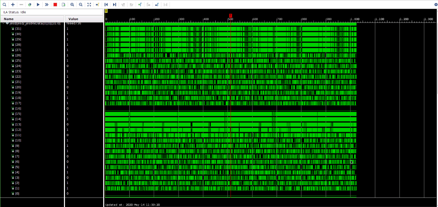
In both cases JESD link is stable.
Please let me know why this behaviour can happen.
I have attached my ADC configuration for your reference. Below are main setting of the ADC.
ADC mode: Mode 0
LMFS: 4841
Sampling rate: 500MHz
DDC: Yes, Fs/4
Let me know if you need any further information.