This thread has been locked.

If you have a related question, please click the "Ask a related question" button in the top right corner. The newly created question will be automatically linked to this question.

AFE4300EVM-PDK: Not working with Mediatek IOT solution AI76x7 over SPI

Part Number: AFE4300EVM-PDK
Other Parts Discussed in Thread: AFE4300

Hi All,

I am working on interfacing AFE4300 (using PDK for evaluation for now) with Mediatek IOT Chipset 76x7 over SPI. The basic problem i am facing is i am not able to read the registers and RDY pin is not getting low to let me read the adc data register. 

Below is brief summary of what i have done so far. 

A. Power [J102 connector of PDK]:-

I am using MMB3 board for powering up the AFE4300 PDK and connected Mediatek Chipset over SPI. Before this i ensured that the PDK is working with provided GUI application from TI.

B. SPI Connections [J103 connector of PDK  ]:- 

1. SPI CLK :- 2MHz (as it is used in AFE4300 PDK)

2. RDY :- Input gpio pin (which is always showing high)

3. RST :- Output gpio pin (working just fine)

4. MOSI :- I can see data on this line.

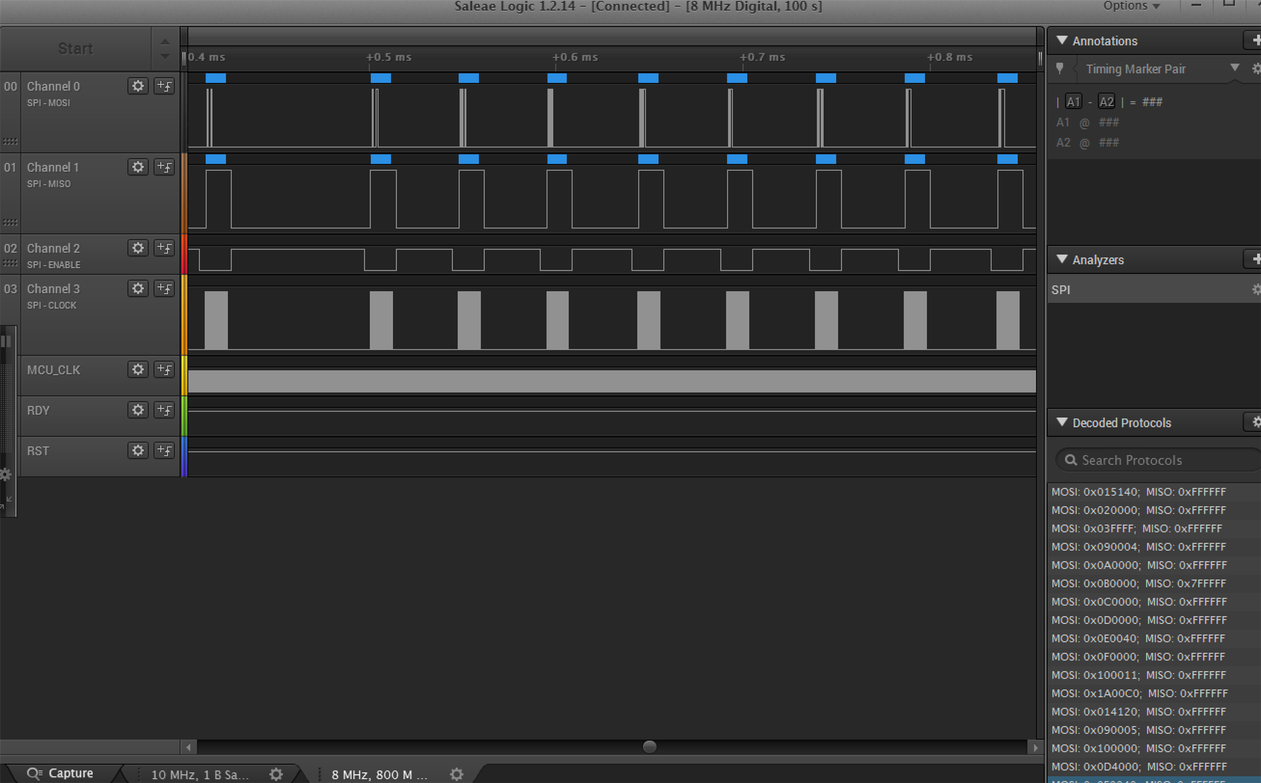
5. MISO :- It is low by default but when write is perform or read is perform during that it becomes high so the output is always (0xffff)

6. STE :- Working just fine as expected to be low during accessing AFE4300 over SPI.

7. AFE CLK :- 1MHz as suggested in the datasheet.

8. GND :- connected to Mediatek Chipset Dev Board ground pin

C. SPI Configurations for SPI controller in Mediatek (using HAL SPI driver provided in Mediatek LinkitSDK 4.5.1v public for 76x7):- 

1. MSB Bit first.

2. SPI CLK -> 2MHz

3. CLK Phase = 1

4. CLK Polarity = 0


D. SW Driver and Testing :-

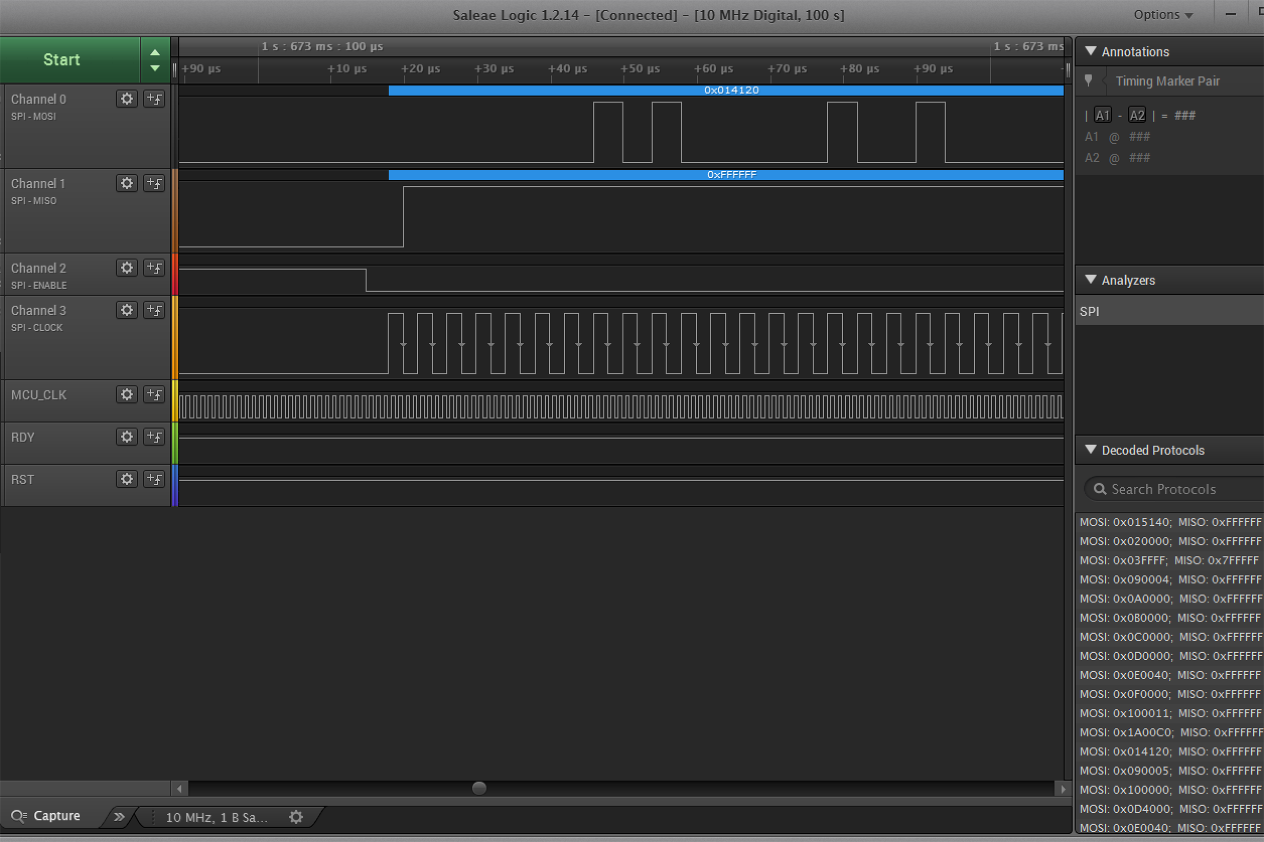
I am able to see over logic analyzer whatever data i am trying to write.

To start with the initialization, i have configured afe4300 registers with the following values :-

 write_reg(REG_ADC_CTRL1,0x5140);

write_reg(REG_MISC_R1,0x0000);

write_reg(REG_MISC_R2,0xFFFF);

write_reg(REG_DEV_CTRL1,0x0004); //Power down both signal chains

write_reg(REG_ISW_MUX,0x0000);

write_reg(REG_VSEN_MUX,0x0000);

write_reg(REG_IQ_MODE,0x0000);

write_reg(REG_WS_CTRL,0x0000);

write_reg(REG_BCM_DAC_FREQ,0x0040);

write_reg(REG_DEV_CTRL2,0x0000);

write_reg(REG_ADC_CTRL2,0x0011);

write_reg(REG_MISC_R3,0x00C0);

Below is the output of logic analyzer :- 

But when i am trying to read the same register it is always as shown in the logic analyzer. Also , when i am trying to read the ADC register for weight measurements after configuring as below mentioned. The ready pin is not changing its state to low.

Configuring for Weight Scale Measurements :-  

  write_reg(REG_ADC_CTRL1,0x4120); //Differential measurement mode, 32 SPS

  write_reg(REG_DEV_CTRL1,0x0005); //Power up weigh scale signal chain

  write_reg(REG_ADC_CTRL2,0x0000); //ADC selects output of weigh scale

  write_reg(REG_WS_CTRL,WS_CTRL_PGA_GAIN(DAC_GAIN_3)); //Gain = 3 DAC Offset = -1

  write_reg(REG_BCM_DAC_FREQ,0x0040); //Frequency = default

  write_reg(REG_IQ_MODE,0x0000); //Disable IQ mode

  write_reg(REG_ISW_MUX,0x0000); //Channels IOUTP1 and IOUTN0

  write_reg(REG_VSEN_MUX,0x0000); //Channels VSENSEP1 and VSENSEN0

I have followed couple of related issues posted in the E2E forum too. 

I would request for help and guidance in this.

Appreciate your help in advance

Thank You

Regards,

Nitish

  • Hello Nitish,

    We have received your inquiry about AFE4300 and will get back to you by next week.
  • Hi Nitish,

    Lets get the register write working first. You can measure the VLDO pin while enabling and disabling the weight scale signal chain.
    Follow the sequence as
    1) Reset the device
    2) Measure the VLDO
    3) Enable the weight scale
    4) Measure the VLDO

    Also can you share the routine for the register read?

    Regards,
    Prabin
  • Hi Prabin,

    Thank you for the quick response.
    I followed the above steps and the voltage i found to be 1.7V when turning on WS Mode.

    I am using Linkit 4.5v SDK provided by Mediatek for this evaluation.
    Below are my read and write functions :-
    //Write Function
    status_t write_reg(uint8_t reg, uint16_t value)
    {
    uint16_t ret;
    hal_spi_master_send_and_receive_config_t tx_config;

    //[SPI Packet : <reg_addr><msb_data><lsb_data>]
    //TX Data buffer
    reg = reg & 0x1f;
    uint8_t tx_spi_data[3]= { (uint8_t)reg, (uint8_t)(value >> 8), (uint8_t)(value & 0xFF)};

    //RX Data buffer- In this case it's zero.
    uint8_t rx_spi_data[3] = {0x0,0x0,0x0};

    tx_config.send_data = tx_spi_data;
    tx_config.send_length = 3;
    tx_config.receive_buffer = rx_spi_data;
    tx_config.receive_length = 3;

    ret = hal_spi_master_send_and_receive_polling(0, &tx_config);
    if (ret != HAL_SPI_MASTER_STATUS_OK)
    {
    LOGE("spi write failed \n");
    return ERROR;
    };
    LOGD("Write:[Tx]:Reg=%.2x,Data1= %.2x,Data2= %.2x,[Write_Val 0x%4x]\n",tx_spi_data[0],tx_spi_data[1],tx_spi_data[2],value);

    return OK;
    }

    //Read function
    status_t read_reg(uint8_t reg, uint16_t *value)
    {
    uint16_t ret;
    hal_spi_master_send_and_receive_config_t rx_config;

    //For reading data from afe4300
    // '1' in bit21 = read operation of reg. 20 = data reg 0
    reg = reg & 0x1f;
    uint8_t tx_spi_data[3] = { (uint8_t)(reg | 0x02), 0x00, 0x00};
    uint8_t rx_spi_data[3] = { 0x00,0x00,0x00 };

    if (reg > REG_MAX_ADDR)
    {
    LOGE("read denied - invalid register\n");
    return AFE4300_ERROR;
    }

    rx_config.send_data = tx_spi_data;
    rx_config.send_length = 3;
    rx_config.receive_buffer = rx_spi_data;
    rx_config.receive_length = 3;

    ret = hal_spi_master_send_and_receive_polling(afe4300_spi_master_port, &rx_config);
    if (ret != HAL_SPI_MASTER_STATUS_OK)
    {
    LOGE("spi read failed \n");
    return ERROR;
    };
    *value = 0x00;
    *value = (uint16_t)rx_spi_data[1];
    *value <<= 8;
    *value |= (uint16_t)rx_spi_data[2];
    LOGD("Read [Rx]:Reg=%.2x, Data1=%.2x,Data2=%.2x,[Read_Val 0x%x]\n",rx_spi_data[0],rx_spi_data[1],rx_spi_data[2],value);

    return OK;
    }

    To turn on WS Scale mode of AFE4300,
    write_reg(0x09,0x6005);
    I am also generating MCU_CLK of 1MHz. With this as i mentioned earlier, i am using power MMB3 board for powering up AFE4300-PDK board.

    Regards,
    Nitish

  • Hi Prabin,

    I figured out the issue. It was actually, the read operation in which i have to add code of writing the register after reading it.So, when i was reading w/o writing again the DEV CTRL register. It was actually erasing the value and powering down the VLDO.

    Thanks once again for your help.
    Regards
    Nitish