This thread has been locked.

If you have a related question, please click the "Ask a related question" button in the top right corner. The newly created question will be automatically linked to this question.

IWR6843AOP: SOP Configuration btw Flashing and Functional Modes

Part Number: IWR6843AOP
Other Parts Discussed in Thread: MMWAVEICBOOST,

Hi TI

There's a question that Customer wants to clarify.

Could you please let us know what is the correct values btw TRM and EVM Guide ?

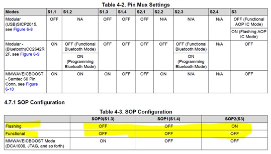
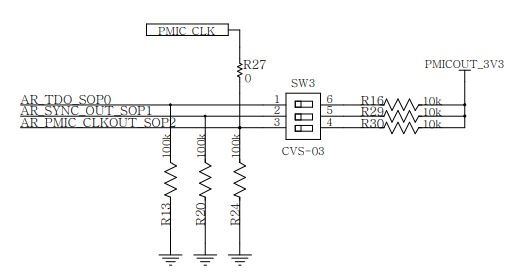
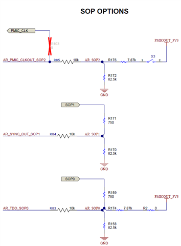
EVM Guide describes Modular-USB, Modular-BT and MMWAVEICBOOST even TRM depicts Bootloader mode as below.

There're different values which are avaiable for Functional and Flashing Mode btw Bootloader mode and Modular mode. 
Please explain differences from the respective modes. 

Regards, 
Jack

  • Hi 


    According to swrr166, When s1.3 is on, it is connected to GND which makes its pin value (SOP0) equals 0.  But for s1.4 , it is contrary.

  • Hello Jack, Ken,

        S1.4 is SOP1 not SOP0.

     Please note There are two different switches S1 and S3. 

    S1 switch controls the SOP0 and SOP1 signals and S3 switch controls the SOP2 signal. 

    Please refer to the below Video link for the the SOP jumper settings for the flash and functional modes.

    Hardware Setup for IWR6843AOP | TI.com Video

    Thanks and regards,

    CHETHAN KUMAR Y.B.

  • Hi Chetan

    I have identified Flashing Setup could be succesful by following Hardware Guide above. 

    But in the Custom board, SOP1 operates differently from TI IWR6843AOP EVM.

    They have to set the SOP0 switch to ON to be Flash Mode in Custom board.

    • IWR6843AOP EVM                  : OFF(SOP0), OFF(SOP1), ON(SOP2)
    • Custom PCB w/IWR6843AOP : ON (SOP0), OFF(SOP1), ON(SOP2)

    They have referred to swrr166a.zip as base design. IWR_ES2 (Rev.F).

    Could you please check if the schematic is different btw IWR_ES2_Rev.F and the hardware which was used in the video training what you gave above?

    Customer still unable to figure out the cause of the problem. Please help on this.

    Regards, 

    Jack 

  • Jack,

       Training video uses same rev F board. Please see the blue circled image in the below screen grab from the above video. 

    Is there a JTAG connected in the system (SOP0 also tied to TDO)? 


    We need to identify the differences between the custom board and TI EVM.

    Also we need to understand the how is the whole system is operated?

    Thanks and regards,

    CHETHAN KUMAR Y.B.

  • Hi Chetan

    Their prototype is almost same with IWR6843AOP-EVM Rev-F. 

    And SOP0 is tied to TDO.

    Customer and I am not able to find out the difference btw Sch.Rev-F(swrr166a) and their Schematic till now.

    5773.Final_T1_6843_AOP_210810a.pdf

    Regards, 

    Jack

  • Jack,

        Thanks for sharing the schematic,  I do see several changes in the schematic w.r.t. to reference design. 

    1) PMIC_CLK net should not connected by default, R27 connects PMIC_CLK net directly this need to be removed. 

    See reference design below:

    Crystal is sensitive to parasitic capacitance, non-symmetrical loading imbalances the oscillator. Hence placement of R109 becomes key and should be close to crystal to avoid any trace parasitic.

    By default this resistor need to be removed.

    See below reference design.

    Care need to be taken, during the power up or power cycling the RF board, DCA1000 board or external emulator should not be connected. 

    Thanks and regards,

    CHETHAN KUMAR Y.B.