This thread has been locked.

If you have a related question, please click the "Ask a related question" button in the top right corner. The newly created question will be automatically linked to this question.

LMT70: T_ON voltage range

Part Number: LMT70

Good day,

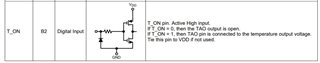
On p.6 of the datasheet, top table, under LOGIC INPUT, T_ON (high) is specified as > 0.66*VDD (typ) with a maximum of VDD-0.5V. 

Does that mean that T_ON must always be ≤ VDD-0.5V?  I.e. it may not be driven up to VDD?  Or does it mean that the threshold of a high level may be as high as VDD-0.5V?

If it is the latter, what is the operational maximum that T_ON may be?  I.e. would it be OK to drive T_ON up to 5V while VDD is only 3.3V?

Best regards,

Rean Bootsma

  • Hi Rean,

    The T_ON threshold of a high level is defined as > 0.66 * VDD and < VDD - 0.5. It is recommended to keep the threshold between these values, in which it would not exceed VDD.

    T_On does however, have an absolute max voltage independent of Vdd of 6V.

    Jalen

  • Hi Jalen,

    Thanks for the quick reply, but technically that's a bit strange.

    So if I supply the LMT70 with 5V, I should not drive T_ON with 5V logic?  I also shouldn't drive it with 3.3V logic, because then it will be tight on the minimum threshold.

    Can you show me the circuit of the input stage (or at least partially) and explain the VDD-0.5V input limit please? 

    Or suggest a sensible way to interface 5V logic to an LMT70 supplied by 5V?

    Best regards,

    Rean

  • Hi Rean,

    Allow me to clarify. The T_ON logic high threshold specification and the maximum voltage ratings should be looked a independently. It's recommended to tie T_ON to the same logic level as VDD to ensure that T_ON is within VDD - 0.5V. If you would like to tie T_ON to a voltage > VDD, it needs to be limited by the absolute max rating of 6V.

    So yes, it could be okay to drive T_ON with 5V logic while VDD is 3.3V although it is recommended to keep these logic levels the same. 

    The equivalent circuit found Pin Configurations and Functions section of the datasheet is all we can provide for the input stage.

    Thanks,

    Jalen

  • Hi Jalen,

    Thanks, that helps.  I did see the partial schematic of the T_ON input, I just was not sure that that is all there is to it.  The VDD-0.5V still does not make sense.  (I did miss the "tie this pin to VDD if not used" part... Sorry. Slight smile )

    How I see it now, is that the limit on the input voltage (on the high side) is due to the characteristics of the reverse breakdown of the diode at the input.  Then the input limit would be absolute, like the 6V from the absolute maximum ratings.  Can you perhaps give me an indication of the input current limit, because then a simple series resistor will quite easily protect circuitry in the case where T_ON is 5V and VDD is 3.3V.

    Or is there some other problem that I do not see right now?

    Best regards,

    Rean

  • Rean,

    All should be good as long as you follow the absolute max limits. This table also indicated not to exceed 5 mA on any pin.

    Jalen

  • Hi Jalen,

    I'm normally not too keen to work with the Absolute Max Ratings, but your answers have helped, thanks!

    Best regards,

    Rean