This thread has been locked.

If you have a related question, please click the "Ask a related question" button in the top right corner. The newly created question will be automatically linked to this question.

IWR6843: Sensors forum

Part Number: IWR6843

Hi altogether,

I am experiencing a similar behaviour as in https://e2e.ti.com/support/sensors-group/sensors/f/sensors-forum/1115651/iwr6843-vbgap-and-vout_14apll?tisearch=e2e-sitesearch&keymatch=IWR6843%20VBGAP

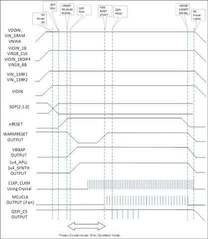
  • After powering up all voltage rails are exact and stable: 3.3V, 1.8V(LDO), 1.2V, 1.0V(LDO) so I proceed in the design checklist: HardwareDesignChecklist_V0p8_IWR6843
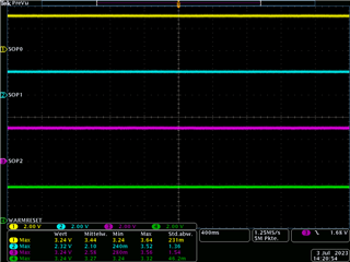
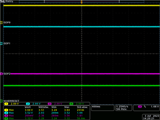
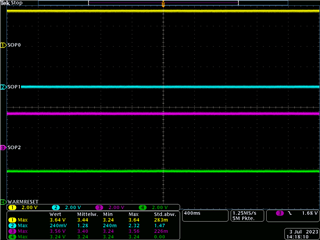
  • SOP mode 2 for development is set: SOP0=3,3V, SOP1=3,3V SOP2=0V
  • Clock is running.
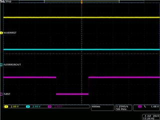
  • N9 WARMRESET is high
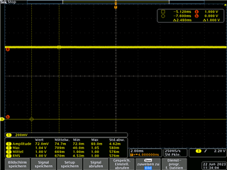
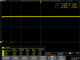
  • B10 VBGAP is approx. 660mV not 900mV as expected
  • A10 APLL, VSYNTH are not 1.4V but only 0.18V - so I expect A14 not to be working either it is at 390mV too low.
  • N6 NERROR_OUT stays low constantly - I suppose there is a cricital error?
  • A reset with NRESET does not change any of the signals - I have two boards with the same behaviour.

As with the post https://e2e.ti.com/support/sensors-group/sensors/f/sensors-forum/1115651/iwr6843-vbgap-and-vout_14apll?tisearch=e2e-sitesearch&keymatch=IWR6843%20VBGAP I tried flashing the device with the MSS/DSS debug file from the mmWave SDK via an XDS110 probe.

  • The XDS110 probe is found at the COM port in windows but I received an error that the serial connection cannot be established.
  • So I ran the probe test in CodeComposerStudio 12 on the XDS - when the target supply is off I receive an error regarding that, so the probe connection itself seems to be OK.
  • With the power supply of the target (IWR) present, I get an error that the JTAG connection is not working. Checking with an oscilloscope the
  • TCK looks good.
  • But the other signals just twitch as if they cannot be pulled low.
  • TDO is overlayed with the SOP0 signal and pulled high by a jumper for SOP mode flashing (101). The signal layout is the same as in the EVM but with 10k both in series and 100k pulldown.

Regarding the connection I followed the XDS target connection guide https://software-dl.ti.com/ccs/esd/documents/xdsdebugprobes/emu_xds_target_connection_guide.html. As the routing length is under 6” I used the unbuffered connection from fig 1. As stated under “JTAG and nTRST Special Considerations (includes TMS and TDI)” pullups on TMS/TDI have been provided as well as an pulldown on TCK and TDO is left as is.

Right now I do not now how to continue in debugging. Any help/hints is thus appreciated.

Best regards

Steve

  • Hi,

    I am forwarding to the correct member of our team, and they will get back to you within 24 hours.

    Regards,
    Tim

  • Hi Stefan,

    Before connecting via UART to run the OOB, we will continue with the hardware debug. The best course of action would be to complete Test 3 and 4 HW bringup guidelines of the hardware design checklist below.

    /cfs-file/__key/communityserver-discussions-components-files/1023/4064.HardwareDesignChecklist_5F00_V0p8_5F00_IWR6843.xlsx

    As you noted, the VBGAP should be 0.9V and not 0.66V; therefore, we can begin further debugging to identify the underlying cause of the problem.  Additionally, make sure the LDOs are functioning properly. I believe the internal LDO may have failed because the probed VOUT_14APLL, SYNTH should read 1.4V. Be sure to probe the 3.3V, 1.2V, 1.0V, 1.8V output supplies to make sure they are operating within the recommended spec limit for power good, This should be fine if you are using PMIC; please double-check. The SOP lines should be stable prior to the NRST release registering the right mode, therefore please verify them as well at the time of reset release (rising edge of NRST). Check that the Warmreset goes from high(1) to low(0) then high(1) within milliseconds at the time of NRST assertion by probing it as well. To identify the cause, you can use the 10 steps listed in Test 3 of the HW bring up instructions. Follow the below wake-up sequencing instructions for proper boot up

    Regards

    Ankit

  • Hi Tim, hi Ankit,

    thanks for the quick reply.

    For the supply the recommended PMIC is used in combination with the recommended LDOs. I measured the switch nodes which are clean and checked the output voltages again. There seems to be no ripple present.

    3.3V OUT (DCDC) 1.8V OUT (LDO)
    1.2V OUT (DCDC) 1V OUT1 (LDO)
    1V OUT2 (LDO)

    Best regards

    Steve

  • Hi,

    In order for the 1.4V SYNTH, APLL internal LDO o/p to come up, you must first complete RF initialization. If you have used the RF INIT calibration API, do let me know. It can be done through mm Wave Visualizer or Studio.

    Regards

    Ankit

  • Hi Ankit,

    no, I haven't used the API I am just following the Hardware Bringup Guidelines.

    Best regards

    Steve

  • Hi Stefan,

    You might try RF INIT and then see whether the 1.4V LDO o/p has come up.

  • Hi Ankit,

    would you please point me to the respective documentation for the RF INIT?

    Best regards

    Steve

  • Hi,

    It shall be done when you flash the appimage through mmWave Visualizer or load the APSS, FECSS firmware through mmWave Studio.

    Regards

    Ankit

  • Hi,

    in my opinion the startup fails at an earlier stage.

    • After turn on voltage rails are stable, see above
    • SOP modes according to swra627 dev mode: SOP2=0V, SOP1=2.5V, SOP0=3V; SOP1 is low but should be sufficient VIH=1.57V
    • NERROR_OUT=3V, WARM_RESET=3V, NRESET=0V
    • NRESET 0V=>3.3V or 3.3V=>0V no change on WARM_RESET or NERROR_OUT, both stay 3V.

    If this basic startup fails, I can only imagine that the chip might be broken. If this is the case I will have to find out the root cause, because I have 3 boards with the same behavior.

    Best regrads

    Steve

  • Stefan,

    A worry is that the warm reset did not change once Nreset was asserted. The N6 NERROR_OUT pin was mentioned as being continuously low in the initial question you posted. Can you confirm this behaviour? Nerror high suggests there isn't a critical error. If you are setting the device in the functional SOP mode, the nERROR may go low for few msec at first powerup (see the MSS#18 in the errata document https://www.ti.com/lit/er/swrz089c/swrz089c.pdf) . and then it would go high again if there no errors.

    (+) AWR1843: Reason why 1.4 V is not output from VOUT_14SYNTH - Sensors forum - Sensors - TI E2E support forums

  • Hi Ankit,

    good point - as you mentioned there can be an CCM-R4F NERROROUT issue with some silicon versions - I am using a different board right now and checked again.

    After applying the supply without any jumpers on the SOP lines - the signals look like this:

    SOP1 is a little low as mentioned 2.3V possibly drawing a litte too much current accross the 10k.

    After pulling SOP2=0V, SOP1=3.3V, SOP0=3.3V with jumpers (Dev Mode)

    or pulling SOP2=3.3V, SOP1=0V, SOP0=3.3V with jumpers (Flash Mode)

    I tried 4 cases:

    1) no jumpers on the SOPs - power the board - wait a few seconds - set SOP for dev mode - wait few seconds - NRESET toggle

    2) no jumpers on the SOPs - power the board - wait a few seconds - set SOP for flash mode - wait few seconds - NRESET toggle

    3) set SOP jumpers for dev mode - power the board - wait few seconds - NRESET toggle

    4) set SOP jumpers for flash mode - power the board - wait few seconds - NRESET toggle

    As the oscilloscope only has 4 channels I cannot show all signals simultaneously - but in any of the 4 cases a toggling of NRESET does not affect WARMRESET as shown below.


    As you can see, WARMRESET stays high constantly as well as NERROROUT. The latter indicating there is no critical error regarding the R4F.

    As soon as possible I will try to cross check the bahavior with a different board.

    Best regards

    Stefan

  • Hi Stefan,

    I was out of office; did you see the same behavior for warm reset with a different board as well?

    Regards

    Ankit

  • Hey Ankit,

    I found an issue in the 1.8V supply rail: some pads were isolated from the rail thus not all voltages were at expected states resulting in the chip not issuing WARMRESET.

    - SOLVED -

    Thanks for your support.

    By the way: there seems to be an inconsistency in the Hardware Bringup Guide / Design Checklist: T3-6 VBGAP voltage check should be a step after the T3.8 WARMRESET voltage check. VBGAP will come up to ~900mV while WARMRESET is in progress as seen below. So measuring VBGAP before WARMRESET is issued will lead to a incorrectly measured VBGAP voltage.

    Best regards

    Stefan

  • Thanks Stefan for your feedback, will work on the Bring Up Guide.

    Regards

    Ankit