


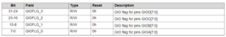
How do ports A, B, C, D, and pins 0-7 in the GIO register correspond to actual chip pins, such as N4, N7, etc?
If you want to use GPIO_ 0. GPIO_ 1. GPIO_ 2. How should the pin function be configured? Is it achieved through the following forms?
Pinmux_Set_OverrideCtrl(SOC_XWR14XX_PINN4_PADAB, PINMUX_OUTEN_RETAIN_HW_CTRL, PINMUX_INPEN_RETAIN_HW_CTRL);
Pinmux_Set_FuncSel(SOC_XWR14XX_PINN4_PADAB, SOC_XWR14XX_PINN4_PADAB_GPIO_0);
The PIN_MUX register information related to the function is not mentioned in the user manual and data manual, so I cannot understand the configuration of this function register in the driver. Is there any configuration information about this function register?
When using GPIO_ 0. GPIO_ 1. GPIO_ 2. Is the control and reading of this pin achieved through the GIO register or PIN_ MUX register implementation?
