Other Parts Discussed in Thread: SN74LVC3G17
Hi,
Q1.
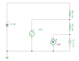
I would like advice on what to look out for when connecting DRV5013 to SN74LVC3G17. We need you to check the external components.
<Conditions>
■ Operating temperature: 5~80°C
■ VCC: 5V±10%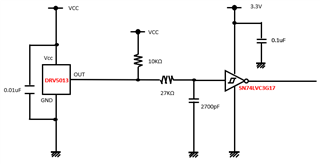
Q2.
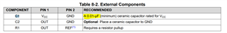
C1 = 0.01uF connected to the DRV5013, but the datasheet indicates that C1 is 0.1uF or more. Which is correct in the data sheet?

Thanks,
Conor