DRV411: design consideration for drv 411

Part Number: DRV411
Other Parts Discussed in Thread: DRV421, OPA454, OPA237, TIPD184

Tool/software:

Dear team,

I am referring to the TI design guide titled ±50A Current Sensor Using Closed-Loop Compensated Hall Element (www.ti.com/.../TIPD180) and have the following queries:

  1. In the design, a 10 Ω shunt is used with the compensation coil, which is correct as per calculations. However, Appendix A mentions a parallel 1 kΩ resistor, making the total resistance approximately 9.901 Ω. Is this parallel network added solely for resistance correction?

  2.  Regarding the 7th point "modification "in the document:
    To design a higher range closed-loop current sensor (±1500 A max), apart from adjusting the shunt resistor value and compensation coil turns/inductance, are there other factors to consider? Can the same PCB layout be used with just component value changes?

    Gain Selection:
    The IC provides three configurable gain modes:

    • Gain 1: 250 V/V, frequency 3.8 kHz
    • Gain 2: 250 V/V, frequency 7.2 kHz
    • Gain 3: 1000 V/V, frequency 3.8 kHz

    My doubts are:

    • On what parameters should the suitable gain mode be selected? The guide suggests starting with Gain 3, but what specific observations or tests should be made?
    • what this gain means what is there role with respect to the compensation coil?
    • The document mentions inductance and core size as critical factors. Are there additional parameters to consider, particularly for determining the gain when designing a wire-wound core?

      I would appreciate clarification on these points. Thank you!


  • Hello, 

    Thank you for your post. 

    1. In the design, a 10 Ω shunt is used with the compensation coil, which is correct as per calculations. However, Appendix A mentions a parallel 1 kΩ resistor, making the total resistance approximately 9.901 Ω. Is this parallel network added solely for resistance correction?

      1. Thank you for pointing this out. This was meant to be a DNP for the 1k resistor.  
    2. Regarding the 7th point "modification "in the document:
      To design a higher range closed-loop current sensor (±1500 A max), apart from adjusting the shunt resistor value and compensation coil turns/inductance, are there other factors to consider? Can the same PCB layout be used with just component value changes?

      1. You are correct for lower current applications. However, without additional circuitry, the DRV411 is not suitable for a 1500A application. Here is a similar post discussing said limitations: (+) DRV411: compensation coil resistance and inductance problem - Sensors forum - Sensors - TI E2E support forums
        1. Larger currents require more secondary windings and/or larger compensation currents.
        2. More secondary windings increase total resistance of the coil.
        3. Increasing gauge wire reduces coil resistance with the cost of a larger core.
        4. Increasing winding and increasing gauge wire may not be enough.
        5. Output drive of DRV411 can be increased with additional circuitry as shown in this post about the similar DRV421 here: https://e2e.ti.com/support/sensors-group/sensors/f/sensors-forum/1035553/drv421-drv421-in--15v-applications 
    1. Gain Selection:

      The IC provides three configurable gain modes:

      • Gain 1: 250 V/V, frequency 3.8 kHz
      • Gain 2: 250 V/V, frequency 7.2 kHz
      • Gain 3: 1000 V/V, frequency 3.8 kHz

      My doubts are:

      • On what parameters should the suitable gain mode be selected? The guide suggests starting with Gain 3, but what specific observations or tests should be made? what this gain means what is their role with respect to the compensation coil? The document mentions inductance and core size as critical factors. Are there additional parameters to consider, particularly for determining the gain when designing a wire-wound core. 
        • This gain essentially is part of the signal conditioning block that controls the Hall sensor spinning currents for the front-end of the DRV411. This is the gain setting applied to the sensed hall voltage and, using gain select, you can choose the appropriate gain setting to ensure loop stability over frequency. This gain setting is determined by the inductance of the compensation coil and size of the hall sensor.
        • Please see the datasheet snippet that I included above. 

    I hope this helps, 

    Joe

  • Dear sir,


    Thank you for the guidance!

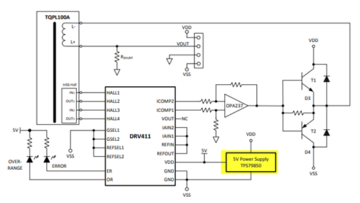
    I now have clarity on the shunt, gain settings, and high-current sensing. I’ve also reviewed the reference schematic for a high-current driver using the OPA454 op-amp, as you  mentioned. Additionally, I analyzed the 100A Closed-Loop Current Sensor design (link:https://www.ti.com/tool/TIPD184), which uses the OPA237 op-amp—a more cost-effective option than the OPA454.

    While reviewing the TIPD184 schematic, I observed several connections to the VSS pin (VSS = -30V max). My understanding is that this pin should be at 0V , which has led to some confusion. Could you clarify the correct connection for VSS?

    Key observations from the TIPD184 schematic:

    1. DRV411 IC: Pins 10, 9, 2, and 3 are connected to VSS.
    2. TPS79850QDGNRQ1 Voltage Regulator: Pins 4 and 9 are connected to VSS.
    3. Passive Components: C1, C2, R5, and R8 are connected to VSS.

    Your insights on this matter would be highly appreciated.


  • Hello,

    I will provide you with an update tomorrow. 

    Thank you for your patience,

    Joe

  • Hello,

    Please see my inline responses:

    While reviewing the TIPD184 schematic, I observed several connections to the VSS pin (VSS = -30V max). My understanding is that this pin should be at 0V , which has led to some confusion. Could you clarify the correct connection for VSS?

    This is a good question. Using the TPS79850 LDO, a 5V supply is created with respect to the VSS voltage. So the VSS can be -15V for example and the supply for the DRV411 would be -10V. This is a floating supply for the DRV411. 

    Key observations from the TIPD184 schematic:

    1. DRV411 IC: Pins 10, 9, 2, and 3 are connected to VSS.
      1. this is the ground connection for the DRV411 and will work for this application. 
    2. TPS79850QDGNRQ1 Voltage Regulator: Pins 4 and 9 are connected to VSS.
    3. Passive Components: C1, C2, R5, and R8 are connected to VSS.

    I believe now that you know that VSS is the GND for the DRV411, the above observations should make sense. 

    I hope this helps, 

    Joe

  • Dear Sir,

    Thank you for your clarification—it helped me understand the schematic better. The concept you introduced regarding the floating load of the voltage regulator was new to me and very insightful! Your guidance has been immensely helpful, and I can now confidently start laying out my PCB based on your suggestions.

    Out of curiosity, I initially considered using the LD1117 voltage regulator to reduce costs, as it is significantly cheaper than the recommended regulator. Would using the LD1117 impact performance? Additionally, would the VSS and ground connections remain the same as in the TPSxx IC, or would the schematic need changes?

    Thanks again for your valuable support.


  • Hello, 

    This is great to hear and I am here to help on anything DRV4xx related :)

    Your regulator question is another important design consideration. 

    Unfortunately, I am not familiar with these two devices as I specialize in the DRV411. 

    I would suggest that you reach out to the group responsible for the LD1117 and the TPS79850 for those trade-offs.  

    I hope this helps,

    Joe

  • Thank you for your kind and helpful response regarding the DRV411. I greatly appreciate your guidance and the time you took to assist me.

    I will connect with the appropriate teams to address my queries about the LD1117 and TPS79850. If I have any further questions about the DRV411, I will be sure to reach out to you.

    Once again, thank you for your support!