Other Parts Discussed in Thread: OPT3007
Hi Team,
My customer used to use OPT3007 to design, but now they change to OPT3006(have pin INT and ADDR).
Now they have difficult about the PCB through hole design for OPT3006.
Please check 3006 spec and find IC package as below data, sensing area size is 0.381*0.298, and the distance between ADDR pad and INT pad is only 0.461, that means the distance sensing area edge to PIN pad is only (0.481-0.381)/2=0.04.
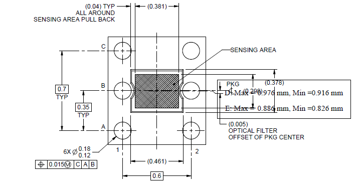
As we know, customers have to consider cutout size tolerance, cutout position tolerance, etc. It is very high risk that sensing area will be shielded, if based on normal design. So, we want to know what is cutout special design for 3006 to lower being shielding risk.
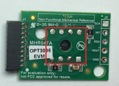
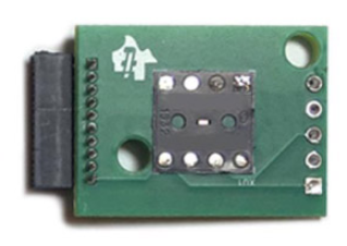
I also send the EVM to customer for reference. If you have more comment, please let me know.