This thread has been locked.

If you have a related question, please click the "Ask a related question" button in the top right corner. The newly created question will be automatically linked to this question.

CD4067B: Individual channels of CD4067B form short path to GND

Part Number: CD4067B
Other Parts Discussed in Thread: ADS8684, LM2904

Hi TI,

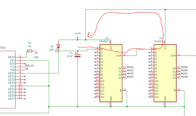
In our application, we're using a series of stacked multiplexers (CD4067B) to multiplex DC voltage from 320 LEDs down to one read from an ADS8684 ADC.  I've attached a simplified schematic showing how this chain looks for one LED.  The CD4067 are powered by a 12V rail, and MUX1 through MUX8 switch between GND and 12V.

The problem we're running into is that individual channels of the CD4067Bs seem to be failing, exhibiting a short path to GND.  Most of the time and for most MUX channels, this system works properly.  We expect almost no current to flow through the CD4067 as they connect the cathode side of the LED (between 0 and 12V) to the [high impedance] inputs of an LM2904 op amp (serving as a differential amplifier).  However, we sometimes observe a substantial (1-2V) voltage drop between I0 of U2 and COM of U2.  This indicates parallel paths to GND for the cathode side of the LED through the PCA9745B (LED controller) inputs and the CD4067B inputs.  This does not happen to all MUXes uniformly, and usually happens to one or a few channels at a time (not the whole MUX).  Replacing the MUX with a new one always fixes the problem.

Given the relatively large capacitor (47uF) on the LED output, the CD4067 inputs will briefly see voltage above VCC when powering the system down.  Is it possible/likely that this would cause a short pathway to form to GND?  Are there other reasons that this might be happening?

Thank you in advance for any help you can provide!

Dan

simplifiedLifetimeV7-1.pdf

  • Hey Dan, 

    So it seems that there is a situation here where the inputs will exceed the VCC of the device. This will violate the abs max operating conditions of the device and can very well cause damage. You'll see in the datasheet that the input voltage range mux not exceed above VDD+0.5 :
    The pathway here would probably not go to ground since the damage would occur on the diode path up to VDD rather than down to GND. That being said, there would still be a current path here.  

    I would try to change the sequencing if possible to power the devices up before applying the I/O signal. 

    Thanks,
    Rami

  • Hi Rami,

    Thanks for your quick response!  We'll implement a new shutdown procedure to make sure we keep all the inputs below VDD+.5V.  Unfortunately, though, I don't think this solves our problem.  As you mentioned, the failure here would cause a current leak to VDD rather than to GND.  Since we're using a current-sinking LED driver and we observe a lower voltage on the COM pin compared to the I0 pin, I think we can be reasonably confident that our failure path is to GND.  Can you think of any type of misuse that could cause a short failure to GND rather than a short failure to VDD?

    Thanks,

    Dan

  • Hey Dan,

    Just an update here. We're currently looking into this to try determine what could be happening here and will have a reply soon.

    Thanks,
    Rami

  • Hi Dan,

    A few more questions if you can help clarify:

    1) What does a short to ground mean? How much current are you seeing on a damaged device? Is it truly a short (no output voltage seen on the device) or is there just a smaller voltage on the output than anticipated?

    2) What does your power up/power down procedure look like? Are you positive the VDD pin is powered before the inputs (can you describe the order you are powering every pin including the logic pins)? Also, like Rami mentioned, this type of failure to GND would most likely be induced if there is an undershoot event (input signal gets pulled -0.5V below ground) or some other overstress event that can cause internal damage (transient event).

    Let me know if you can help provide these details and we can further help debug this.

    Thanks for your cooperation.

    -Bryan

  • Hi Bryan,

    1)  When I say a short to ground, I mean that there is a smaller voltage on the output than anticipated.  In our case, our VDD is 12V, the voltage on I0 is ~10V, and the output would have something like 7.5V

    2) Our power up procedure gives ~15V from a power supply to a linear regulator set to output 12V.  This 12V provides power to logic-level linear regulators (3.3V).  Our logic is provided by an FT232H USB bridge (powered at 3.3V), whose outputs drive MOSFETs to facilitate the voltage shift from its logic level (3.3V) to the MUX logic level (12V).  The gates of these MOSFETs are pulled low by pulldown resistors to ensure that their outputs don't float before the logic pins are actively low or high.  On the input side of the MUXes, the LED driver will attempt to drive 0mA through the LED.  This means that the inputs voltage ends up somewhere between ~7-11V (1-5V below the 12V VDD).

    Power down cuts power to all of these at once, so the capacitance in the system will dictate voltages on each device.  Most of that capacitance is in the 47uF capacitors between 12V and the LED inputs.  We do not have transients of the 12V power on each of the relevant locations, but can investigate these if you think this could be the source of the problem.

    Thank you again for your help!

    Dan

  • Hi Daniel,

    Appreciate the extra details here. The large discrepancy between the VDD cap and the input cap would mean that the inputs would likely not discharge nearly as fast at the VDD and there would be an overvoltage condition during this power down. I would suggest making that capacitor smaller or match the VDD cap if you can. If there are multiple shutdowns before the problem presents itself, the device could be getting incrementally damaged by the overvoltage events seen during this sequencing. The damage would manifest itself as this increased current through the I/O to VDD path and the voltage drop across the typical 120ohm resistance of the multiplexer would make sense for that reduced output voltage. 

    I know you mentioned you believe the short is to GND, but I am not sure that is the case. You could be damaging the 2nd CD4067 as well and that would allow excess current to flow through the 1st CD4067 and cause that large voltage drop as the current is flowing through the VDD of U3 (and could flow back through the LED current path instead of through the supply).

    Let me know if that helps and makes sense.

    Thanks!

    Bryan

  • Hi Bryan,

    I think we may have found the issue, and it's what you and Rami have both been suggesting.  I want to apologize to both of you: I made a subtle but major mistake when redrawing this simplified version of the schematic.  C1 (47uF) should be between VDD and the input I0 (see attached corrected picture), NOT between the input and GND.  This does make it so that the input can be pulled below GND when the setup is powered off.   I think this is why we're seeing a short failure towards GND.

    And while I agree that the current path you drew above is a highly likely mode of failure for that circuit, I think the excess current flow through U2 would lead to a higher voltage on the output, not a lower voltage?  Regardless, I suspect we have found the actual culprit thanks to your help!

    8508.simplifiedLifetimeV7-1.pdf

    Our current plan is to put a diode between the negative leg of the capacitor and GND to act as a clamp, preventing C1 from pushing the input below GND level.  I'll report back to the forum regarding whether or not this works just in case anyone else stumbles across this in the future.

    Thank you both again for your help!

  • Hi Dan,

    Not a problem! Glad we could come to a resolution on this. Please reply if you would like to share your findings as you mentioned.

    Let us know if you have any other questions.

    Thanks!

    Bryan