This thread has been locked.

If you have a related question, please click the "Ask a related question" button in the top right corner. The newly created question will be automatically linked to this question.

TMUX1511: TMUX1511 related issues

Part Number: TMUX1511

hi,

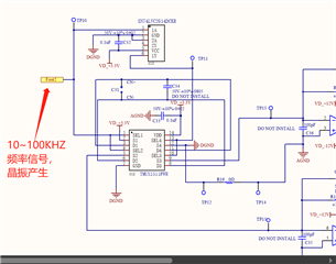
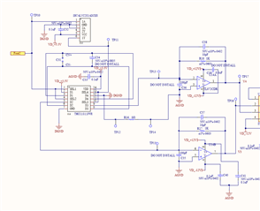
Fout2 inputs a frequency square wave from 10KHZ to 100KHZ, and SEL1 and SEL2 are both high or low levels. SEL3 and SEL4, due to the connection of inverters, have opposite levels to SEL1 and SEL2. When SEL1 and SEL2 are high, 3.3V is used to charge the C31 capacitor and collect current through U14B (TL072CDR) integration. C31 is a capacitive pressure sensor, which is now simulated with a 1pf capacitor. The frequency change output sampling should have changed, but there is no change now. Please help analyze the reason. The schematic diagram is shown below;

Thanks!

  • Hello Zhang,

    Just want to clarify some things in the design to fix the problem

    1.What is the voltage of the FOUT signal. I understand the frequency 10 -100kz but what is the voltage of that signal?

    2. What is the voltage  of the signal going into the sel3 and sel4 pin.

    If you refer back to the answer from Stephen on the original post their are other design problems that i think we can fix and  have this circuit operate properly 

    "Also the connection on the TMUX1511 is from S to D. Currently all your D pins (D1-D4) are all floating and shorting to the other pins. So based on your setup, S1 (3.3V) can connect to S4 (0V), and S2 (TP15) can connect to S3 (TP13). Those are all the connections available. 

    The S1 to S4 connection you need to be very careful about because this will violate the max current through the switch and cause possible damage, if both S1 and S4 are on at the same time. I recommend limiting this current with a resistor. 

    And your S2 and S3 pins will never see a higher voltage since they are always floating." 

    Can you share some description on what you are trying to achieve or maybe an example waveform? Then maybe we can suggest a more optimal circuit setup. 

    Thanks,
    Stephen 

    -Stephen

    Please let me know if you can implement and send over some of the information stephen asked for?

    Regards,

    Kameron

  • HI,

    1. The voltage of the FOUT signal is 3.3V,Square wave signal;

    2. When the FOUT pin inputs a high level (3.3V), the SEL3 and SEL4 pins output a low level (0V). When the FOUT pin inputs a low level (0V), the SEL3 and SEL4 pins output a high level (3.3V);

    May I ask if the signal can go from D to S?

  • Hello Zhang,

    Could you please provide us some additional information through waveforms of the circuit operation. 

    Can you please share the voltage signals at TP10, TP15, and TP16 during circuit operation. This information will help us understand if the integration circuit is working the way you expect it to.

    Thank you,

    Jacob