A related question is a question created from another question. When the related question is created, it will be automatically linked to the original question.
If you have a related question, please click the "Ask a related question" button in the top right corner. The newly created question will be automatically linked to this question.
TS3A227E: Asking for the TS3A227E schematic review
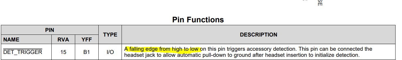
My main concern is note 12 with the DET_TRIGGER pin. The current schematic has opposite operation. You can place an inverter in between the phone jack switch and the DET_TRIGGER pin or choose a phone jack with the switch with the opposite operation.
1. VDD is correctly supplied with 3.3 V which is within the recommended operating conditions and includes bypass capacitors.
2. SCL and SDA are not used correctly tied to VDD
3. MIC_PRESENT is open drain output is correctly pulled up with a resistor.
4. MIC_P correctly connected to codec
5. INT# is not used and correctly connected to ground
6. GNDA for FM support features not used and correctly grounded
7. GND_SENSE is not used and correctly connected to ground
8. GND correctly connected to ground
9. SLEEVE and SLEEVE_SENSE correctly connected to sleeve of the phone jack
10. RING2 and RING2_SENSE correctly connected to Ring 2 of phone jack
11. Tip pin is correctly connected to the tip of the phone jack.
12. DET_TRIGGER pin to initiate the automatic detection sequence is not connected correctly. The phone jack looks like it has a normally closed switch that is connected to ground. This connection will pull the DET_TRIGGER pin low when no headset is in the phone jack. When the headset is insterted into the phone jack the phone jack switch will open and the DET_TRIGGER pin will go high due to the internal pull up of the TS3A227E. This operation is opposite of the required operation stated in the datasheet.