This thread has been locked.

If you have a related question, please click the "Ask a related question" button in the top right corner. The newly created question will be automatically linked to this question.

CD4051B-Q1: Demux voltage range for motor control application

Part Number: CD4051B-Q1
Other Parts Discussed in Thread: DRV8847, , SN74CBT3251, MUX507

Hello, I'm trying to search for a 1:8 demux from TI.

I use MSP430G2 launchpad to generate PWM signals (10 ~ 10kHz, 1~60% duty cycle) and this is connected to a motor driver DRV8847 to control brushed DC motors.

I'm using 20V power supply to power the motor driver.

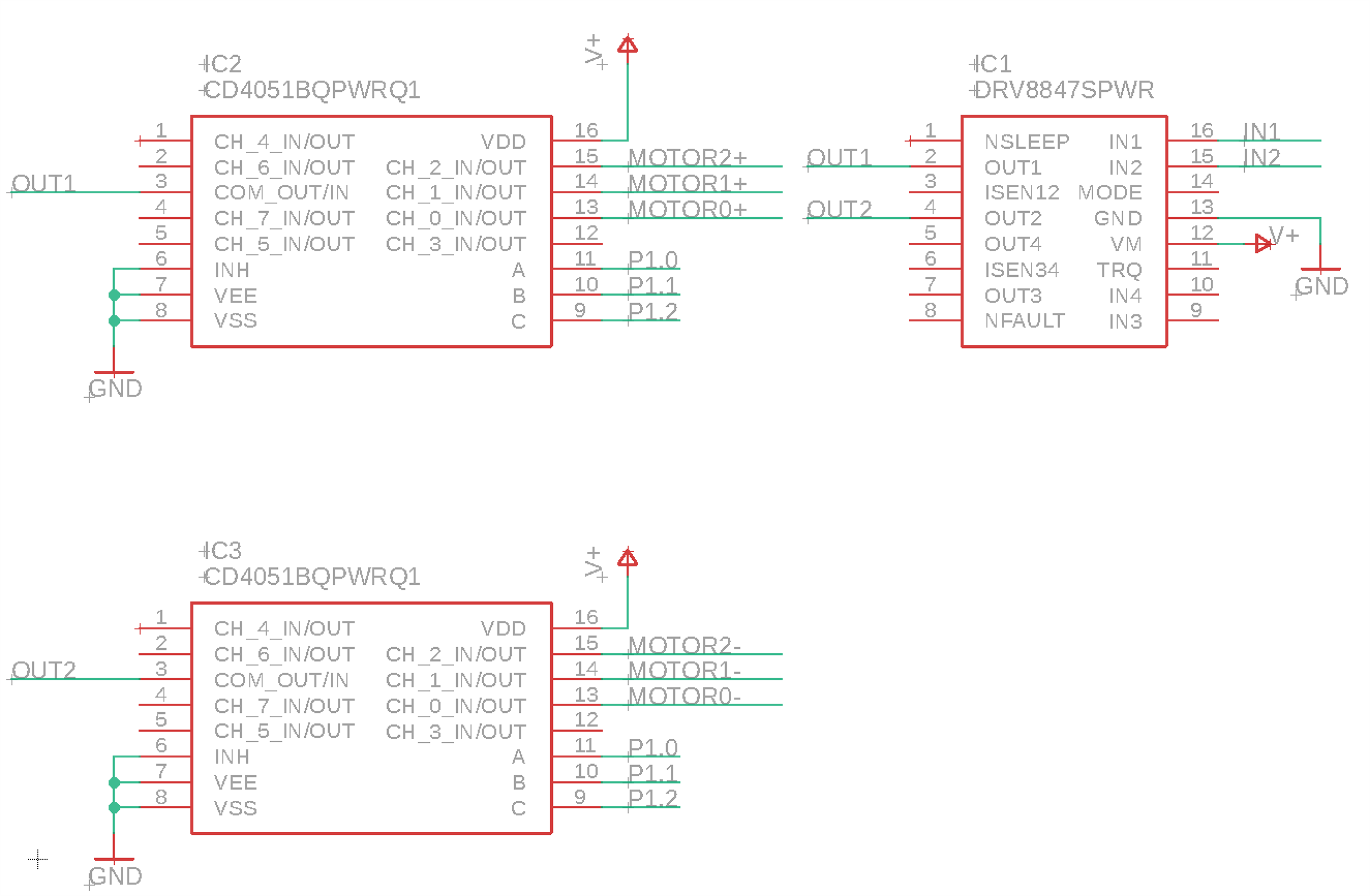
I have 8 DC motors to control. Instead of populating multiple motor drivers, I wanted to use a single motor and use two 1:8 demux to reroute the PWM signals.

May I ask

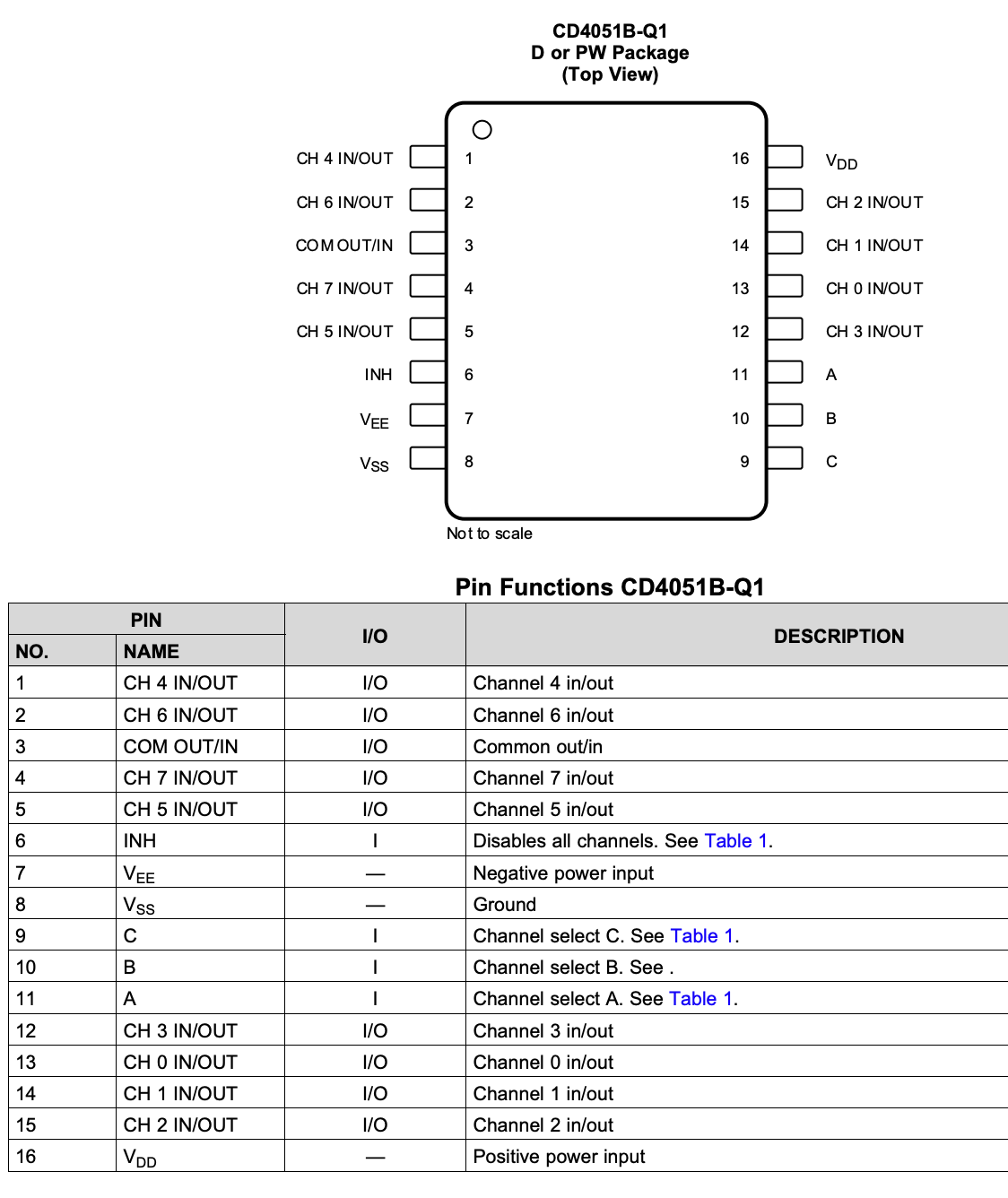
Q0. Can I use two CD4051B-Q1 (CD4051BQPWRQ1; one for each DC motor pins) to choose which motor to run with a single 20V motor driver?

I noticed CD4051B-Q1's max supply voltage is also 20V.


Q1. The MSP430G2 has 3.3V GPIO. Can I control CD4051B-Q1's input channel A/B/C with the 3.3V GPIOs when supplying 20V to CD4051B-Q1?

I hope I'm following the voltage rating correctly.


Q2. Can I set VEE=VSS=GND for my case?

Q3. Pin 3 - COMMON IN/OUT; is this the data input pin, for my case the 20V PWM signal goes here?

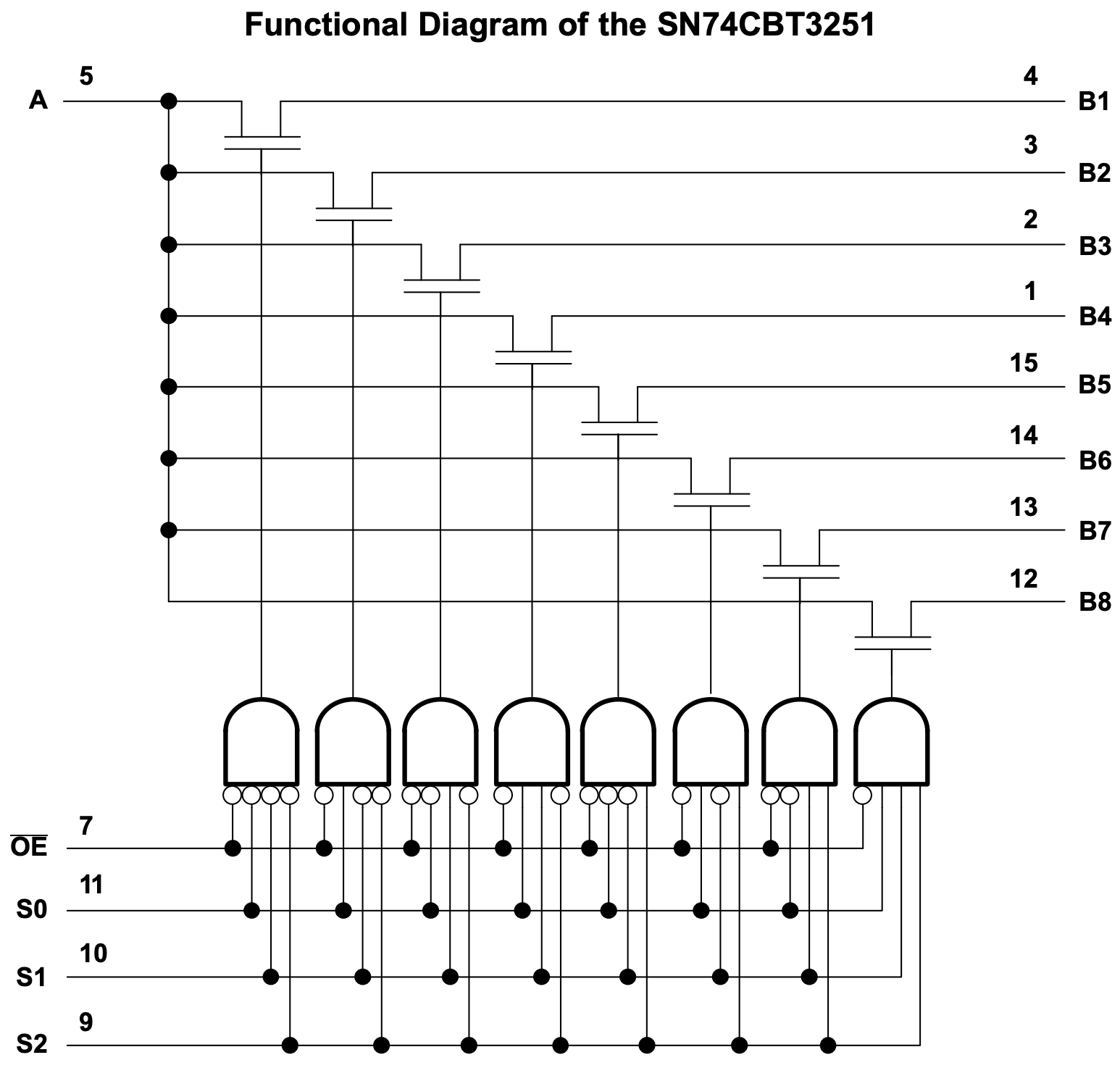
Q4. Referring the SN74CBT3251's functional diagram (NAND gate + N Channel MOSFET), does CD4051B-Q1 also have the same configuration as well?


  • Hello David,

    Could you please send a more detailed diagram of your system? I am trying to better understand how you would like to use the two CD4051B-Q1 muxes. Would you like to use them to switch the PWM signals at the input of the motor driver or to switch the motors at the output of the motor driver?

    What is the maximum current draw of one of your motors? The absolute maximum DC input current of CD4051B-Q1 is 10mA.

    I would like to point out that 20V is the absolute maximum rating for both CD4051B-Q1 and DRV8847. Please see the note about Absolute Maximum Ratings below:

    Stresses beyond those listed under Absolute Maximum Ratings may cause permanent damage to the device. These are stress ratings only, which do not imply functional operation of the device at these or any other conditions beyond those indicated under Recommended Operating Conditions. Exposure to absolute-maximum-rated conditions for extended periods may affect device reliability.


    To answer a few of your questions:

    Q1. Control inputs A/B/C are not compatible with 3.3V logic levels when using a supply voltage of 20V. For example, the VIH minimum at 15V supply is 11V.

    Q2. You may set VEE=VSS=GND.

    Q4. CD4051B-Q1 does not have the same functional diagram configuration as SN74CBT3251. The architecture of CD4051B-Q1 uses transmission gates, while SN74CBT3251 uses NFETs.


    Regards,

    Kate

  • Dear Kate

    I was trying to mimic this figure for my motor application.

    The DC motor spec - it is a toy car motor

    https://www.adafruit.com/product/711
    Rated Load: 10 g*cm
    No-load Current: 70 mA max
    No-load Speed: 9100 ±1800 rpm
    Loaded Current: 250 mA max
    Loaded Speed: 4500 ±1500 rpm
    Starting Torque: 20 g*cm
    Starting Voltage: 2.0
    Stall Current: 500mA max

    In my case, the max current needed is 10mA per DC motor.

    I hope this conceptual schematic helps; although you've mentioned the max current and A/B/C are not compatible with 3.3V logics,

    by using the same A/B/C data, I wanted to choose a motor using the CD4051B-Q1

    I hope you understood what I'm trying to do.

    Again from Q3, is the COMMON pin the data pin? I need to give the 20V PWM signal to the demux.

    Also, if the CD4051B-Q1 cannot be used, would you recommend an alternative?

  • Hi David,

    Thanks for sending that information.

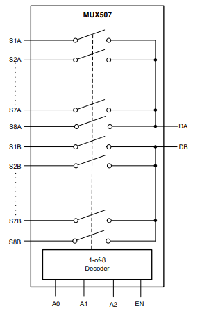
    I think you can accomplish this with one dual 8:1 mux, MUX507, instead of two CD4051B-Q1.

    MUX507 supports a higher voltage (recommended up to 36V) and channel current (recommended up to 25mA). The digital input pins (A0, A1, A2, EN) are compatible with 3.3V logic levels.

    Below is the functional block diagram for MUX507:

    DA and DB should be connected to your OUT1 and OUT2 channels, respectively.

    SxA pins should be connected to your MOTORx+ and SxB pins should be connected to your MOTORx-.

    Regards,

    Kate

  • Thanks for your recommendation, Kate.

    Few more things before closing this;

    Kate Dickson said:
    The digital input pins (A0, A1, A2, EN) are compatible with 3.3V logic levels.

    Q0. That is great news for me. Where can I get the electrical voltage limits for the A0, A1, A2 pins?

    Q1. In other words, do you think the analog output pins (S1A, S8B, etc) are fine when connecting an inductive/capacitive load like the DC motor?

    I wish the motor won't damage the analog output pins.

    Q2. Lastly, about the VSS, I need to connect GND to VSS directly, right?

    However, that seems to contradict with the decoupling capacitor, which should be populated between VSS and GND.

  • Hi David,

    Q0. Logic input voltage levels can be found in the Electrical Characteristics: Single Supply table on page 9 of the MUX507 datasheet. According to the table below, the minimum value for a logic input to be counted as a "High" (VIH) is 2.0 V and the maximum value for a logic input to be counted as a "Low" (VIL) is 0.8V. This is standard for 3.3V logic levels.

    Q1. The mux is designed to function within the recommended operating conditions. If these conditions are exceeded, operation is not guaranteed. Make sure you stay within these conditions for this device.

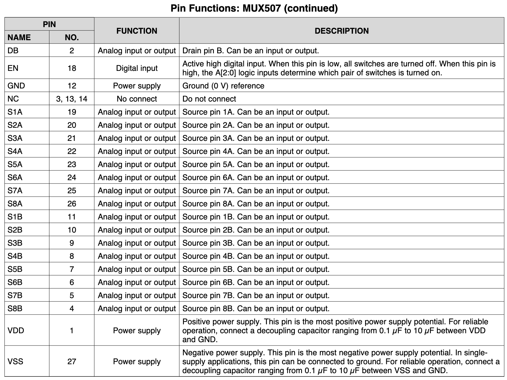
    Q2. The Pin function table states for VSS, "In single-supply applications, this pin can be connected to ground." The mention of a decoupling capacitor applies to the configuration when VSS is connected to a negative voltage supply.

    Regards,

    Kate

  • Kate Dickson said:
    The mux is designed to function within the recommended operating conditions. If these conditions are exceeded, operation is not guaranteed. Make sure you stay within these conditions for this device.

    You mean like the maximum voltage ratings? Or is there polarity issues/off-leakage current requirements I have to be aware of?

  • Hi David,

    I am referring to the Recommended Operating Conditions, such as supply voltage, source and drain pin voltage, and channel current. These can be found in the Recommended Operating Conditions table of the datasheet. Make sure these operating conditions are met for this device.

    Off-leakage current specifications can be found in the Electrical Characteristics table.

    Best Regards,

    Kate