This thread has been locked.

If you have a related question, please click the "Ask a related question" button in the top right corner. The newly created question will be automatically linked to this question.

SN74CB3Q16211: SN74CB3Q16211

Part Number: SN74CB3Q16211

Hi,

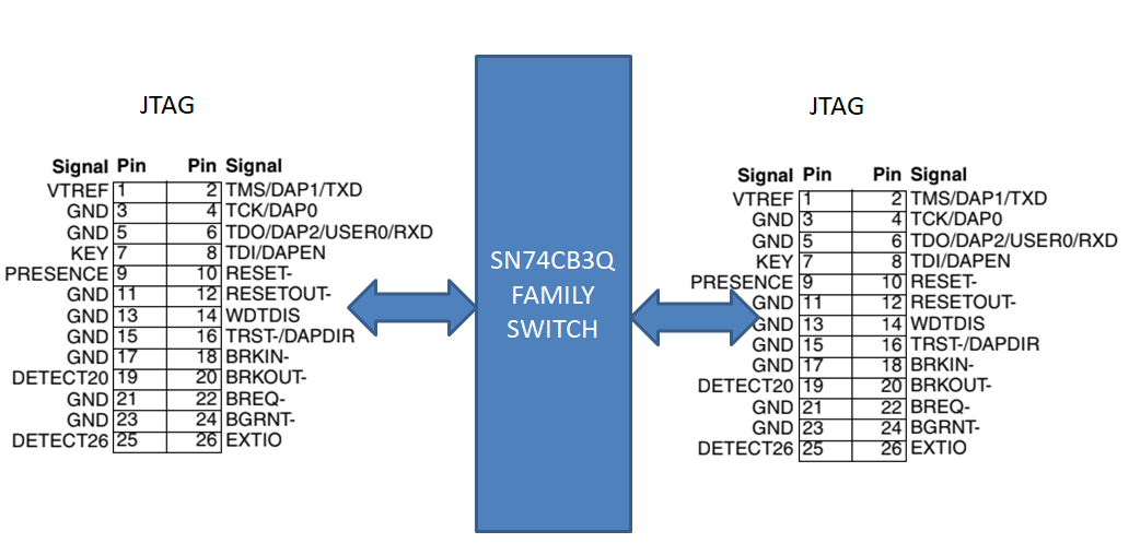
We have an application where we want a switching mux like device for connecting a master JTAG debugger (debug connector) to multiple slave debug (connectors) .

consider the following application circuit. I am thinking switching also the VCC and GND signals.

I see the absolute maximum rating of continuous current through the channel. But I dont see the max value for recommended operating conditions. What is the max power dissipation of each channel switch?

Is the above application possible with switch? If not Could anyone also recommend another switch that suits my application.

Thanks,

Shrikant

  • Hi Shrikant,

    Could you please upload the images again  so we can help you with your questions- they are not showing up in the thread above.

    Regards

    Saminah

  • The absolute maximum rating of 64 mA is the allowed current. The switch itself does not care and will still work, but the rest of your circuit might not be able to handle the voltage drop of 64 mA × 5 Ω = 320 mV over each switch.

    Why do you want to disconnect GND?

  • Hi Saminah,

    Thank you for your response. Please see the attached file. I have put basic idea of switching the JTAG pins.

    Best Regards,

    Shrikant

  • The reason behind this idea is that, if you see the JTAG debuggers, every manufacturer of debugger has their own signals (apart from main JTAG main signals) and also, the signals are assigned to different pins of their connectors. So, if I want to design the switching circuit for different debuggers then, there is lot of complexity involved and nearly not possible (considering the PCB size, cost  etc. etc.). So, I just do not want to worry about all these and simply pass all the signals (and so, I want to separate GND of debugger lines from control GND circuitry) through this switch.

    So, I just wanted to know if I can use this switch assuming the target controllers are powered externally (not from debugger) which means, the current requirement from target controller is given by other source and does not pass through the FET switch.

    I chose this IC because I read on page 15 in the application note http://www.ti.com/lit/an/scda008/scda008.pdf?ts=1588165714086 that, we can use such switch for PCI bus. So, I thought PCI bus contains VCC, GND signals similar to JTAG and hence I can use that. But, nothing is explicitly mentioned in this application note.

    Thanks in advance.

    Shrikant

  • Hi Shrikant,

    What is the supply voltage and signals you are passing through the switch? 

    As Clemens mentioned,  the maximum allowed current for the e SN74CB3Q16211 is  64 mA.  It depends on your application circuit if it can handle the voltage drop across the switch and cause issues reading the signal downstream.

    Do you need a 24 channel or more for your application?

    Regards

    Saminah

  • Hi Saminah,

    Thank you for your reply.

    The signal that pass through this switch are JTAG signals like TMS, TCK,  TDI, TDO, GND, VDD(3.3 or 5v max). If you look at my application block diagram I have put a sample JTAG debugger connector with the signals. This is from lauterbach debugger.

    As far as I understand the datasheet of SN74CB3Q16211 it is mentioned that, it has charge pump and so the drop is almost negligible and it provides rail to rail switch. So, I don't think I should be worried about the voltage drop at each pin. Am I right or I have understood it wrong ?

    Again thank you for your response.

    Regards,

    Shrikant

  • The charge pump means that the switch resistance does not much depend on the signal voltage (a FET increases its resistance when the source voltage nears the gate voltage). So the SN74CB3Q16211's resistance is flatter than that of other FET switches (but not perfectly flat; see figure 1). It's still 5 Ω, which should be fine for any digital signal.

  • Hi,

    Now I understand what you mean. So, if I use other power source to power the target controller instead of the VDD from debugger itself (so that, I need not worry about 320mv drop on VDD line) then, I think it can be usable in our application right?

  • Yes, this should work.

  • Hi Clemens,

    Thank you very much.

    Best Regards,

    Shrikant

  • Hi Shrikant,

    What are common switch architectures? video has  more details on how different switch architectures include with NFET with charge pump.

    Please let me know if you have any other questions.

    Regards

    Saminah