Hello,
I am using the SN74CB3T3306DCUR to connect a 3.3V I/O to an signal that could be up to 5V. I need to be able to either receive a 3.3V or 5V signal OR transmit a 3.3V signal. I have this part's VCC connected to 3.3V and the OE# pins tied to ground. The B terminals are connected to my device and the A terminals go to connectors so that a signal may be cabled in or out.
The problem that I am seeing is the output voltage at the B terminal is low when there is a 3.3V signal on the A terminal input from the connector.
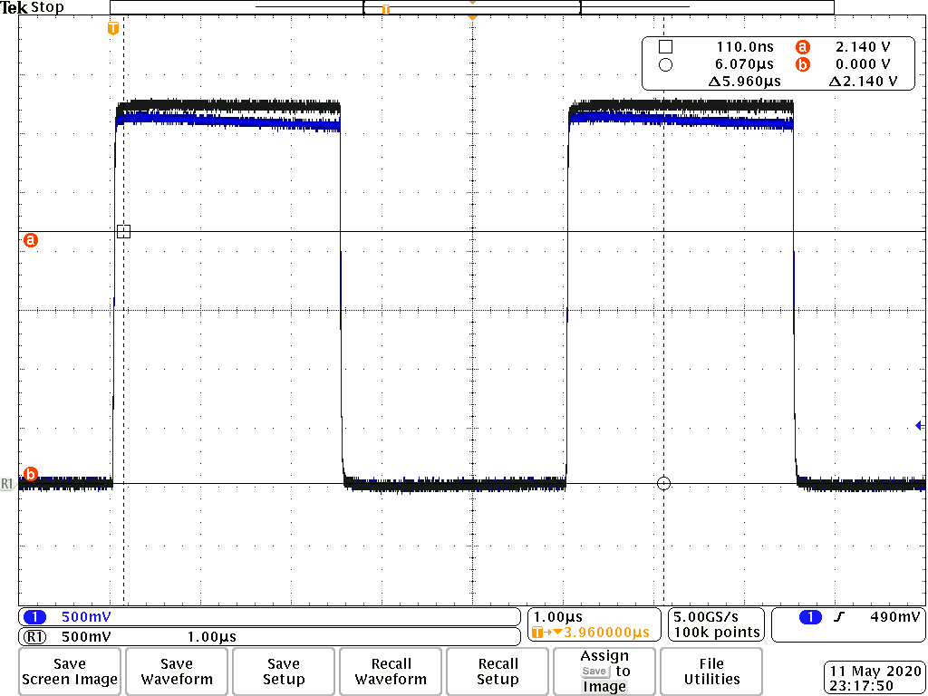
The image below shows my input signal. The dark gray waveform is the 3.3V signal incident upon the A terminal measured at the A terminal. The blue waveform is the signal output at the B terminal and measured at the B terminal using the same probe.

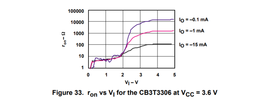
The signal initially rises to the correct level but then gradually falls to about 2.1V. There is a 10k pull-down at the input of my device on the B terminal side of the bus switch. While this functions, I would like to understand why the signal drops to this level. From the datasheet, I would expect this signal to be close to VCC with current less than 1mA. Have I misunderstood the datasheet about this part?
Do I require a pull-up on the B terminal?
Now, when I drive the B terminal with my device, I get a reasonably good signal on the A terminal. If you look at the scope capture below, the dark gray trace is the 3.3V signal driven on the B terminal by my device and measured at the B terminal. The blue trace is the signal at the output A terminal measured at the A terminal. The signal is loaded with an oscilloscope set to 1 MOhm input.
This signal gradually drops to about 2.95V, which is more acceptable. Why does it behave differently in this direction?
Thanks for your help.