This thread has been locked.

If you have a related question, please click the "Ask a related question" button in the top right corner. The newly created question will be automatically linked to this question.

CCS/TMDSEMU200-U: hardware connection problem between TMDSEMU200-U and 66AK2G12 (CCS "test connection" fails)

Part Number: TMDSEMU200-U
Other Parts Discussed in Thread: 66AK2G12,

Tool/software: Code Composer Studio

To whom it may concern,

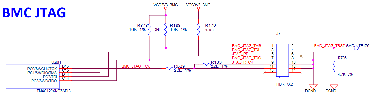
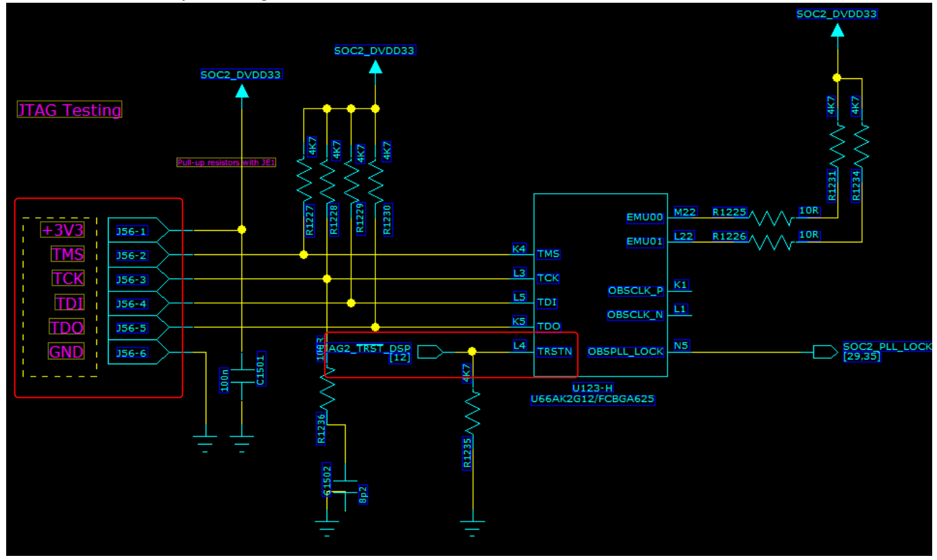
Following is the schematic of JTAG connection on our prototype board. After several modification of the prototype board, we still couldn't pass the CCS "test connection". Is there any similar design that we can use as a reference?

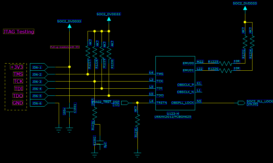
The hardware changes we've made are:

(1) make the TRSTN on K2G "high"
(2) connect the nRESET pin of XDS200 to "high" (doesn't change anything in the CCS error message)
(3) connect the TDIS (GND) pin of XDS200 to GND (change CCS error message from -183 to -233)
For the XDS200 pin definition please refer to http://support.spectrumdigital.com/ccs53/xds2xx/files/xds200_quickstart_guide.pdf

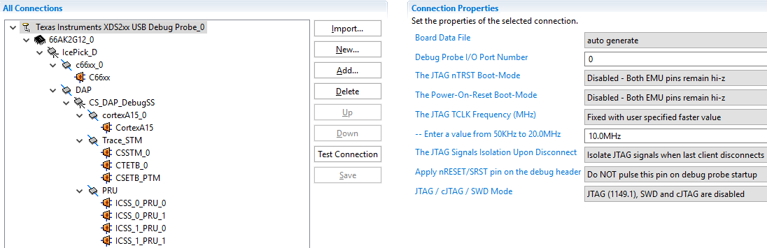
When using CCS "test connection" I chose "Texas Instruments XDS2xx USB Debug Probe" for "Connection", and "66AK2G12" for "Board or Device". The CCS version is 8.0.0.00016.
We've checked this "Debugging JTAG" manual: http://software-dl.ti.com/ccs/esd/documents/ccsv7_debugging_jtag_connectivity_issues.html
And the "XDS Target Connection Guide - Design guidelines for JTAG": http://dev.ti.com/tirex/#/?link=Development%20Tools%2FDebug%20Probes%2FXDS%2FDocuments%2FXDS%20Target%20Connection%20Guide

We also tried to connect the XDS200 to "CPLD JTAG" on K2G EVM board with the same 6 pins on the schematic and TDIS (GND), and got the same error (-233). However we were able to pass the "test connection" if we plug the XDS200 to the BMC JTAG on K2G EVM using the "TI14 Adapter".

At this point we are wondering whether we can have some reference schematic design of the connection between XDS200 and any DSP SoC, using only the most basic pins (GND, TDO, TDI, TCK, TMS, VTRef).

Thank you,
YW

  • YW,

    The XDS Target Connection Guide you linked is the best reference we have for the JTAG design. You could also look at the K2GEVM schematics for details on how the connector is tied to the device. 

    That said, I am curious: why haven't you connected the singals TRSTn, EMU0 and EMU1 of the 66AK2G12 device to the XDS200? The TRSTn pin resets the JTAG state machine (which in certain devices this is critical for establish a connection) and the EMUn pins set the mode of the JTAG state machine (which may influence the ability to connect).

    Even with this conifguration, I would start by opening the Advanced tab of the Target configuration file and see if the TCLK clock is set to "fixed" and try to reduce its speed to establish the connection. If you are able to connect at a very reduced speed, this indicates the lines are suffering from severe noise, delays, or are slow enough still make the TJAG state machine to work without the TRST signal.

    If you still can't connect, I would try to modify the circuit and add the connections I mentioend above. It goes without saying that I am assuming the connections are actually ok - i.e., there are no disconnects due to soldering or PCB routing.

    Hope this helps,
    Rafael

  • Hi Rafael,

    According to our hardware engineer, nTRST on XDS200 is currently drived to high by nRESET on XDS200, which is connected to Vcc. And TRSTn on K2G is pulled to high. Therefore we didn't connect nTRST on XDS200 directly to TRSTn on K2G. Does that makes sense to you?

    For EMU0 and EMU1, we're not using them as showed in the following picture. Besides, the BMC JTAG on K2GEVM doesn't connect EMU0 and EMU1 either and the "test connection" still passed. Therefore I don't think EMU0 and EMU1 have to be connected to XDS200 in our case.

    For the TCLK clock settings I've tested the following but all get the same error (-233)

    Fixed with user specified faster value - 10MHz/1MHz/1KHz
    Adaptive with user specified limit - 10KHz

    What do you think?

    Thank you,
    YW

  • Hi Rafael,

    We just modify our JTAG adapter to pull the EMU0 and EMU1 to Vcc. So now EMU0 and EMU1 pins on both the XDS200 side and the K2G side are pulled to Vcc. And we still get the same error (-233).

    Thank you,
    YW
  • YW,

    Thanks for sending the target configuration screenshot. A few comments/questions:

    - The reduction in TCLK speed in your configuration helps confirm the problem is in connections themselves and not (completely) noise or delays. They may still exist, but the pressing problem is actually disconnected wires.  

    - The nTRST signal is different than the nRESET signal. The nTRST in certain targets is necessary to reset the JTAG logic (I can't find the spec for the K2G device to tell you if this signal is absolutely required). Given the K2GEVM connects this signal to the SoC device and it works, why the change in your prototype?

    Following the K2GEVM schematics: the MIPI_TRST# signal goes to a buffer (U132) and a switch (U134) which becomes the net SOC_TRST#. That net is pulled low but is also driven by the JTAG Debug Probe.

    In your schematics I don't see J56 (which I assume is the JTAG connector coming from the TMDSEMU200-U) driving this line.

    - The BMC JTAG on the K2GEVM goes to the TM4C device and not to the main SoC, which are radically different devices. Where you able to do a successful Test Connection on the MIPI-60 pin connector that goes to the SoC? I suspect you will be successful, but it wouldn't hurt to try.  

    - What is the host OS you are using? Is this a native or VM? Operating through a VM imposes additional problems to the connecting process.

    - According to the schematics you sent initially, the EMU pins of the SoC were already connected to Vcc and they match the K2GEVM schematics, thus I am not entirely sure what were the modifications performed in your last post. If you simply connected the EMU pins coming from the TMDSEMU200-U to Vcc, that would not have much effect given the Debug Probe drives these signals. That is fine as it is. 

    - Just to be sure, I would use an oscilloscope, check the JTAG waveforms and compare to what is shown in the post below. Although they deal with a different device, there is a chance this may uncover any problems. 

    https://e2e.ti.com/support/tools/ccs/f/81/p/661170/2442314#2442314 

    At this point I can't think of any additional topics to check, but I will definitely report back if I find something else that may be relevant. 

    Hope this helps,

    Rafael

  • Hi Rafael,

    Our hardware engineer has modified the hardware according to your suggestion. It doesn't change the outcome. However we found the TCK signal problematic as showed in the following two pictures (low signals not low enough to be read as 0). They were taken when "test connection" in CCS is performed. We even unplug the TCK pin from our prototype board and got the same result. Do you know what could cause this behavior? We're still trying to get a MIPI-60 to CTI-20 adapter so we can verify the integrity of this XDS200 JTAG.

    I also took measurements of TMS to guarantee that I used the correct voltage display setting of the oscilloscope:

    Thanks,
    YW

  • YW,

    Sorry about the delay; i was out of the office yesterday.

    I don't know what could be causing the high level on TCK, but it certainly can be tied to a strong pull up (if the TMDSEMU200-U works flawlessly in another board). Looking again at your schematic I would lose R1228 and R1236, which will in turn disconnect C1502. Despite these resistors are populated on the original K2GEVM board, they are not part of the Target Design reference.

    software-dl.ti.com/.../emu_xds_target_connection_guide.html

    Perhaps the reason why these resistors were put in the K2GEVM is that they are connected to a 245 buffer (U123) which is probably stronger than the combination output buffers + the long JTAG cable of the TMDSEMU200-U.

    I would also remove R1227, R1229 and R1230 for the same reason.

    Apart from this I am running out of ideas. Hopefully this will help move closer to a solution.

    Rafael
  • Hi Rafael,

    Thank you for the response. Before we proceed modifying the board, may I confirm this first?
    "We even unplug the TCK pin from our prototype board and got the same result." => in this case will modifying the resistors/capacitors on our board change the clock signal from TMDSEMU200-U?

    Thanks,
    YW
  • YW,

    Please apologize again for the delay; last week I was out of the office.

    I am not sure if you were able to overcome this, but I missed the question highlighted by you above.

    Given you unplug everything and the TCK signal is still at around 2.4V, I suspect the voltage divider between R1228 and R1236 is the responsible for that. The TCK is an input from the standpoint of the device.

    Regards,
    Rafael
  • Hi Rafael,

    No worries. However there is a misunderstanding of my description. I apologize for the confusion. In my post which have 4 oscilloscope results, we used the connection suggested by you. "We even unplug the TCK pin from our prototype board and got the same result." means we only disconnect the TCK pin between XDS200 and our protoboard, but all the other pins remain connected.

    If I unplug everything the "Test connection" in CCS wouldn't proceed to the point that I can measure TCK signals.

    Please let me know if the above description is not clear.

    Thank you,
    YW