This thread has been locked.

If you have a related question, please click the "Ask a related question" button in the top right corner. The newly created question will be automatically linked to this question.

TIDA-01527: Questions to resolver feedback winding monitoring

Part Number: TIDA-01527
Other Parts Discussed in Thread: TL431, OPA322-Q1

Hello all,

 I'm designing a resolver circuit for motor control, according to the reference design "TIDA01527" I have several questions.

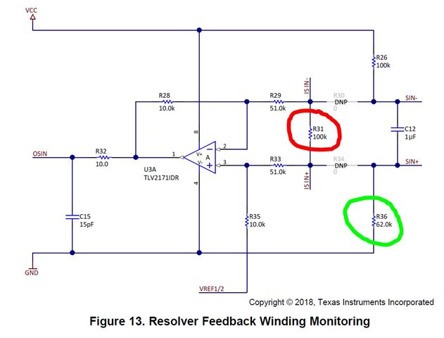
Question 1: Why the DC biasing resistor R36 = 62k, why not the same like R31 and R 26 = 100k?

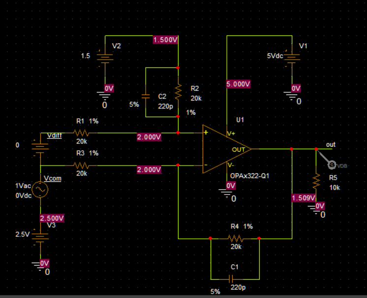
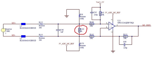
Question 2: In this case, the resolver feedback winding runs very small current,  shouldn't we increase the load current of the resolver feedback winding so that it may get more noise-resistance? For example, we want to reduce the R31 to 1k, to let the resolver feedback winding runs a litter bit more current like over 1mA.. (see our design below)


So what do you think is this a good idea or just superfluous?

I would be very grateful if you guys could help! Thanks you!

BR

Jin

Jin

  • Hello Jin, this is Jiri, the author of the TIDA-01527.

    I must admit I don't exactly remember why the resistor divider is not symetrical. You practically need to make sure that the input signal does not clip and the voltage on input pins of the operational amplifier does not exceed the input common mode range. Just put your circuit in a simulator and check if it stays within the limit.

    Regarding the resistor - what you say makes sense to me but I do not have any practical experience with it. I suggest you check the resolver specification what is the maximum acceptable loading impedance.

    Regarding you circuit - make sure that the Vref 1.5 is a stable voltage reference that can sink and source current. This must NOT be a voltage divider. TL431, or a resistor divider with an opamp for buffering, does the job. I am bit worried about capacitors C45 and C60 in your circuit. Theoretically, they create a low-pass filter. However, it is important that the impedance of both networks is identical over the frequency range. Capacitors come with relatively high tolerance even if they come from the same reel. Mismatch between the networks ruin the common mode rejection ratio. Just try try to do an AC analysis for the common mode rejection for 5% caps mismatch.

    I am now out of the office but try to support you with your request as quickly as possible. Please accept short delays. 

    Kind regards, Jiri

  • Hi Jiri

    Thanks a lot for your reply.

    Without C45 and C60 then this circuit might be unstable, cause the small phase margin.

    Why did you say " Mismatch between the networks ruin the common mode rejection ratio."? I don't understand that. CMRR is a inferent atrribute of a OPA correct??

    I also noticed in your design, after the output of the opa(U3A), you putted a very weak LP filter, R32(10) and C15(15pf), could you please tell me the purpose of this LP filter?

    Best regards,

    Jin

  • Hi Jin, I am back in the office again.

    Let me please address first the common mode rejection ratio topic. The purpose of a difference amplifier is to eliminate the common mode noise (ground shift). An ideal operational amplifier has an infinite CMRR. However, the output of a real operational amplifier reacts slightly to the input common mode voltage change. The CMRR parameter defines how good or bad this behavior is. Once we expose the amplifier to the external circuitry the common mode rejection of the CIRCUIT may change. Attached is the monte-carlo simulation of the difference amplifier. Resistors have 1% tolerance, capacitors 5% tolerance. The thick green trace is the nominal run that corresponds to ideal parts. This correlates with the OPA322-Q1 datasheet.
    The rest of the waveforms are random tolerances. You can see that the common mode rejection drops down to 30 dB around 30kHz. This is also a common switching frequency of industrial motor drives. 

  • The weak low-pass filter is something we call "a charge bucket filter". When the sample and hold circuit triggers, there is a short current impulse that charges the sampling capacitor. Some opamp configurations do not react to this event well and exhibit a transient with damped oscillation, overshoot, etc. If this transient event takes longer than the S/H window, the ADC result is compromised with an error. You can nicely measure it with an oscilloscope, ideally with an active probe and using the proper high-frequency measurement techniques.

    More details on the subject is here:

    https://training.ti.com/ti-precision-labs-adcs-final-sar-adc-drive-simulations-lab

     I hope this helps.

    Kind regards, Jiri

  • Hi Jiri

    Thanks you very much for the Info.

    We use 0.1% resistor and 5% COG capacitor for 10kHz automotive application, it should be ok I hope?

    Btw, could you please tell me how can you use this circuit to measure the CMRR? How can you get the Aol (differential gain) value?

    BR

    Jin

  • Thanks for this tips.

    My problem is we don't use separate ADC, but direct the ADC of a TMS320F2837xD Dual-Core Microcontroller, it's very difficult to calculate the best RC-setting.

    Now I just use a 47 Ohm and 10nf, what do you think about this setting?

    If it isn't ok, could you please tell me which value should I use?

    Thanks again!

    Cheers

    Jin

  • Hi Jin,

    I find 10nF capacitance unnecessarily big.  You may see issues with the OPAMP stability. For the charge bucket filter we typically use tens of picofarads. That's why I have 15pF and 10 ohm in the previous design. ADC S/H circuit characteristic for the TMS320F2837xD is here: https://www.ti.com/lit/ds/sprs880o/sprs880o.pdf?ts=1665390811761&ref_url=https%253A%252F%252Fwww.google.com%252F

    page 107.

    Please note that not all channels have the same input capacitance (Refer to the table 8-8).

    Kind regards, Jiri