This thread has been locked.

If you have a related question, please click the "Ask a related question" button in the top right corner. The newly created question will be automatically linked to this question.

TIDA-010042: Clarifications on Reference Design

Part Number: TIDA-010042
Other Parts Discussed in Thread: CSD19531Q5A, LM5109B, MSP-FET

Hi Team,

Our customer has a couple of questions regarding TIDA-010042:

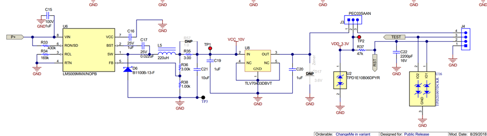
1. Why are R45, R45, R55, R56, D8, D9, D10, D11, D12 and D13 not supposed to be populated?

What are the use of R45, R46, R55, R56, D8, D9, D10, D11, D12 and D13?

I read the technical data but it did not explain why those components are DNP.

2. Do you also have CSD19531Q5A and CSD18540B for TO-220 package Version? According to the schematic, I can get 40A by swapping the MOSFET to TO-220 version.
If you don't have them, may you recommend which MOSFETS I can use in the design that have the same characteristics as the CSD18540B and CSD19531Q5A.

3. Do you have a video related to TIDA-010042 programming? I have built 3 of them and I want to test for 12VDC, 24VDC and 48VDC for my project. However, I'm experiencing difficulty on how to get the system up and running while connected to the battery and Solar panels (that delivers 30VDC). I'd appreciate if there is a video showing how to connect the solar, battery and load to get the feeling on how it works before programming the MCU. We would appreciate if you could help us on where and why to connect the pins on the jumper connectors. They are very confusing.

Thanks in advance!


Kind Regards,

Jejomar

  • Hi Jejomar,

    Thanks for reaching out. Please find my answers below:

    1. These parts are optional place holders, which are not mandatory to operate this design. R45, R46 R55 and R56 allow to tie the gate to ground in case there is no defined output signal at the gate driver output. For example if it is not powered. D8,D9 D10 and D11 would allow for a faster turn off, since they allow to bypass the gate drive resistors for turn off. D12 and D13 should be placed according to the schematic. A detailed explaination why this diode is necessary can be found in the LM5109B datasheet ( https://www.ti.com/lit/ds/symlink/lm5109b.pdf ) in chapter 7.5.
    2. Yes, the referred TO-220 parts are CSD18542KCS and CSD19531KCS
    3. There is no video available for how to setup. You can follow the instructions in the Design Guide.

    Best regards,

    Andreas

  • Hi Andreas,

    Many thanks for the answers. It was really helpful. We would appreciate your help on our customer's follow-up question:

    Before I began any programming of the MSP430, I tested points on the J2 designator pins that are supposed to read VCC_3.3V by connecting pins 1 and 2 (since the solar panel is used to supply the voltage to the MCU) and the J1 designator pin that is supposed to read VCC_10V, however, designatorJ2 reads 2.5VDC while at the same time, pin 8 at designator J1and TP1 reads 0VDC. The solar panel supplies 30VDC, therefore, how can you help me solve this issue? If the respective pins' output voltage is not according to the datasheet, then what are your recommendations? I am sure, before programming, the respective pins are supposed to at least output 3.3VDC and 10VDC, but since they are not, then I would definitely need your help.

    Kindly note that I did not use 45° rather I used an arc to make corners on the board, therefore, is that why the readings at pins 1 and 2 read 2.5VDC?


    Kind Regards,

    Jejomar

  • Hi Jejomar,

    The shape of the corners should not have any influence on these voltages. You should be able to read 10V at TP1 and 3.3V at TP2.
    Please also make sure the that the right pins of J3 are connected with a jumper. For debugging you can connect pin2 and pin 3 to use the 3V3 provided by the debugger.

    Best regards,

    Andreas

  • Hi Andreas,

    Sorry for the late reply, I was going through the PCB design today. R57 and C45 were the cause of the problem since they are marked DNP. After removing them from the PCB, the circuit worked as it was intended, that is, TP2 read 3.3V (actual values were between 2.99V~3.31V) and TP1 read 10V (actual values were between 9.98V~10.01V), which is normal due to components parasitic values.

    At the moment, I have not programmed the MCU as I am waiting for the MSP-FET device bought from TI to arrive to start programming, however, when I tested the voltage at the battery terminals, it read 2.55V and at the load section, it read 0.00V, therefore, should I first program the MCU before connecting the battery (battery section to read 24V) and load for it to work? There is absolutely no voltage or current readings at the Load terminal and the charging current and voltage output at the battery are very small.


    Kind Regards,

    Jejomar

  • Hi Jejomar,

    Glad to see the circuit working now.

    Yes, the MCU needs to be programmed before connecting a battery or a load, since it controls the buck converter. Depending on what batteries and loads are connected the software needs to be modified. In general I recommend to have a close look at the code. It is more an example how the design can needs to be control, than a full application software.

    Best regards,

    Andreas