


Other Parts Discussed in Thread: PMP11065
Hi,
in the flyback converter reference designs PMP11107 and PMP11065 the author implemented a self-driven secondary rectifier:
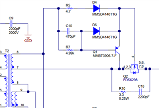
It works reasonably well in situations where one does not want to employ dedicated ICs. But I am struggling a little to fully understand the circuit. My musings so far:
- In principle I think Q1 is used to quickly rush out the gate charge from Q2 to turn it off.
- R7 limits the static base current of Q1 to some quiescent level, and C10 provides an AC path for a much higher current peak to speed up the switching of Q1.
- D6 might be there to protect the base-emitter junction of Q1 from being excessively reverse-biased (might otherwise die at some 6V or so).
- R5 and D4 then seem to provide the turn-on path for Q2.
Does that remotely make sense?
Thanks a lot & kind regards,
Sven
