Because of the holidays, TI E2E™ design support forum responses will be delayed from Dec. 25 through Jan. 2. Thank you for your patience.

This thread has been locked.

If you have a related question, please click the "Ask a related question" button in the top right corner. The newly created question will be automatically linked to this question.

PMP11329: Loop oscillations- LM5021-1

Part Number: PMP11329
Other Parts Discussed in Thread: LM5021, UC3844

Hello,

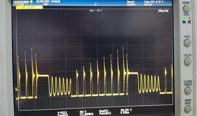
I'm using the TI reference design PMP11329 for one of my power supply design with the output of 18V, 3.6A. I'm able to get till 2A of output but the drain waveform oscillates or the entire loop. The drain waveform looks like below. Switching frequency is currently 100kHz. Initially I tried with 150kHz also.
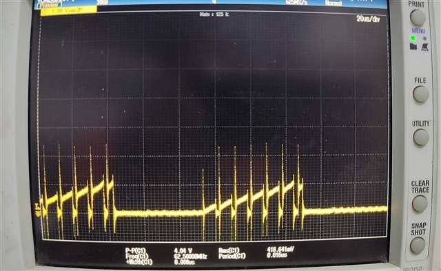
And my current sense waveform looks like below with 500mohm sense resistor.
Kindly help me to solve the issue. Thanks.

  • Hi Saravanan,

    Can you please share the schematic. Sometimes these issues are hard to debug remotely. It could be a layout issue or a wrong component as well. 

    Did you follow the PMP11329 design exactly?

    Thanks,

    Robert 

  • Hello Robert,

    Thanks for your reply.

    I followed the schematic of PMP11329 as much as possible. You can have a look at the attached schematic.

    Below is my top and bottom layout.

    Top


    Bottom

    Kindly suggest a solution.

  • Hi Saravanan, I have asked one of our engineers to take a look and suggest some ideas here. Please give us some time.

    Thanks,

    Robert 

  • Hi Robert,

    Thanks for your response. Will be looking forward for your suggestions.

  • Hi Saravanan,

    Is the 2A current limit consistent across the input voltage range? I am having a hard time reading the schematic, but what is the current loop set to? Can you test with that loop disabled?

    Thanks,

    John

  • Hi John,

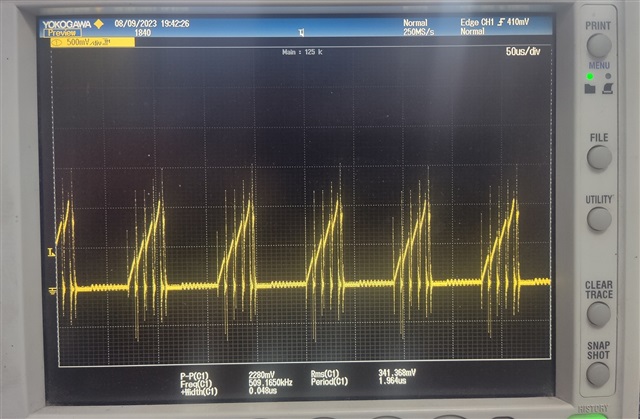
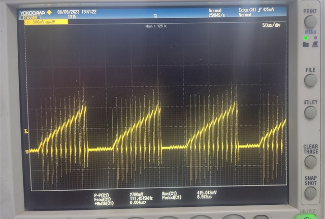
    2A current limit seems to be same for different input voltages. Below are the snapshots.

    According to the reference design, the current loop filter cut off frequency is 146kHz (4.02K & 270pF) which I tried initially. I tried with 3.8kHz (4.02K & 10270pF) also by increasing the CS pin capacitor. I tried reducing or increasing the slope compensation.

    Thanks

  • It sounds like something happening on the secondary side since it happens across the input range at the same loading point.

    Is it possible to test the board without the circuit by U2? That might be limiting the current and sending the IC into a restart cycle.

  • Hi John,

    Forgot to mention that U2 is already disabled by removing R11. U1 also is disabled. And in place of Q1, I put a Schottky diode to test out if that was an issue. I doubt secondary side since the current limit is consistent across different input voltages. May be a layout issue but before redoing the layout, I want to confirm what part is causing the issue. Anything else I could try or I'm missing something? 

    Thanks

  • It might be the layout, having the controller span the PCB makes the CS signal susceptible to noise and may weaken the gate driver.

    Can you check the drive signal to see if noise is coupling in? On PMP11329 the LM5021 and external driver are right next to the low-side fet Q4 which helps with performance.

    For the current sense i would increase the series resistor and lower the capacitance?

    Also, can you upload a schematic that is easier to read? So that I can make more specific recommendations.

  • Hi John,

    There is no noise in the gate drive when the loop is open. I tried with UC3844 and it worked. Maybe LM5021 is more sensitive to noise and layout. As per spec, LM5021 is superior and can aid high performance and efficiency. I'm planning to make two different boards with these two ICs. Looking for the points to improve in the layout. Clearer schematic is attached. Let me know your comments.

    Thanks

  • Hi Saravanan,

    UC3844 has an OCP level of 1V while LM5021 is 0.5V. Did you scale the current sense resistor to correlate with the change in device?

    In the applications section of LM5021 (8.2.2.6) equation 22 uses roughly half of the max Vocp level to correlate with the maximum expected primary peak current. This provides a good amount of signal for the control loop while having margin for the OCP.

  • Hi John, 

    Though I didn't change the Rsense for UC3844, I tried earlier with 1/5 of the current Rsense for LM5021. 

    Right now I'm somewhat convinced that it's an layout issue due to which there is oscillation. But I don't know which section or what to improve 

  • It is not ideal to have the CS trace span the board, but it seems like that is the only way to route that section and have the FETs set to the bottom edge of the PCB.

    The routing for the CS trace seems okay, having it run next to the ground plane is a great way to minimize the loop inductance. I think the only thing you can change is the filtering by the controller.

    If I am reading the layout correctly, it looks like the Ccs goes through two vias before returning the the GND pin of LM5021. This extra inductance may be enough to allow the noise to trip the OCP. in your PCB can you flip the cap so that the ground connection is directly to the GND pin of LM5021? Below is a drawing to show where it might make sense.

  • Hi John,

    Thanks for your suggestions. Earlier I tried by flipping the capacitor and soldering one end directly to the IC pin. It didn't help though. But implementing the same in the layout might help. I'll consider this and try to bring down the IC as far as possible to reduce the trace length and stray inductance.

  • Vias can also act as antennas and pick up noise so it would help to reduce the number of this on sensitive nodes as much as possible.

    Additionally here is a link to an article that I find useful, it goes through the various considerations when designing a layout.

    https://www.ti.com/seclit/ml/slup230/slup230.pdf

  • Hi John,

    Thank you for your suggestions.

    I'll redo the layout with both the ICs. I'll come back if there is an issue.