This thread has been locked.

If you have a related question, please click the "Ask a related question" button in the top right corner. The newly created question will be automatically linked to this question.

TIDA-010062: Test Setup for Labs

Part Number: TIDA-010062
Other Parts Discussed in Thread: PMP41006,

Hello,

To test the PMP41006 for 'Lab1' 

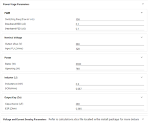
As mentioned in Section 3.1.1.3.2 of the design guide, the DC input voltage(upto 120V) is given at 'J7' for 'Lab' tests.

Need clarifications where exactly the 120VDC has to be applied? Since J7 will hold the for GaN daughter card.

Regards,

  • Any update on  this?

    Regards,

  • Hi,

    Sorry for confusing. TIDA-010062 design files were changed after this design guide. Please ignore the name of 'J7', the 120VDC should be powered on the (AC) input port. 

    By the way, there is a known bug during DC input testing, A small DC bias (10V~20V) is needed before the code run to start the power stage, (too high DC input may cause OC protection too). Otherwise, bacause of an oppoiste zero voltage drift, the MOSFET leg may short the input port.

  • Hello,

    Thanks for the much needed clarification and heads up on the DC input testing bug.

    Soon planning to do all the "4 lab tests" for the PFC Stage by following the steps mentioned in Section 3.1.1.3.2 and providing DC input at the AC input port with 10V/20V DC Bias.

    Please let me know about any other known bugs/steps missing in the document to prevent the test from facing avoidable errors and damaging of the components.

    Regards,

  • If you want to do Lab3 testing, the control won't startup before Vac higher than 75Vrms. And, load should be CR mode (Const Resistance) with 150 ~ 500ohm, neither too high nor too low.

  • Really appreciate this.

    Thanks,

  • May I know why the Power and Vbus values are not as per the TIDA010062 design in the main.syscfg page?

    [Power is specified 3300(instead of 1050W), Vbus is specified as 380(instead of 385V)]

    - Currently I want to test the board as it is. So is it safe to proceed towards all 4 Labs by debugging with the above(default) values?

    - Also I could not find the calculations.xlsx for this design in Resource Explorer. Kindly share the same, if its missing.

    Regards,

  • small DC bias (10V~20V) is needed before the code run to start the power stage,

    I am testing Lab1 as per section 3.1.2.5.1  of TIDUET7G with a DC Bias of 12V before starting the code run as you mentioned above. 

    At no load with 12V input, observed Vbus was around 21V. 

    However as mentioned in the document after providing 500Ohms CR Load from initial condition for Lab1, the boost operation stopped after 15V. (i.e getting 16Vbus for 16Vin and so on)

    What might be causing this?

    Regards,

  • You can change it as your wish, I don't know why this value is changed.

  • This is not right, if you put 12V input, the output should far below 12V before generating PWM pulse. You may add a 0.2A load, to avoid some charge come from space.