This thread has been locked.

If you have a related question, please click the "Ask a related question" button in the top right corner. The newly created question will be automatically linked to this question.

TIDA-010042: Issue for high side gate signal from driver

Part Number: TIDA-010042
Other Parts Discussed in Thread: LM5109

Hi,

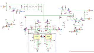
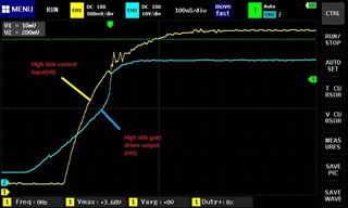
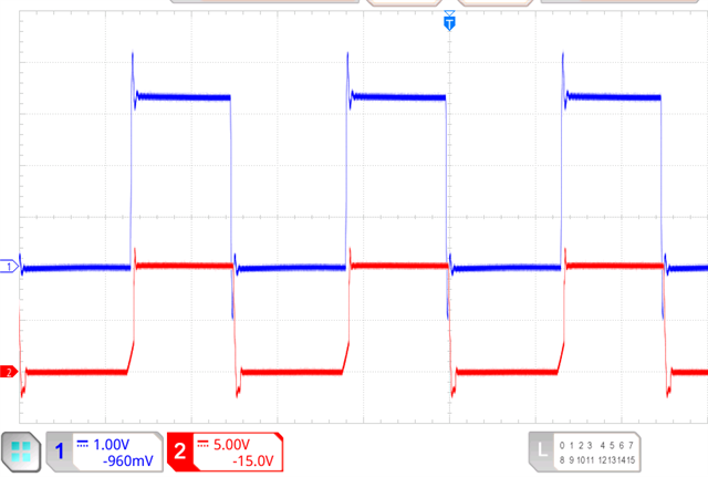
I am developing a battery charger based on TIDA-010042 old reference design(not GaN reference design)  with slight modifications. Please see the attached schematic of interleaved buck . While testing the hardware, I have observed that high side gate driver output from driver LM5109 is starting before the HI signal from the microcontroller and there is rise time of . Waveform is also attached. But this issue is not seen for the low side gate output. Low side gate driver output is perfectly following the low side control input from microcontroller. To verify, I have tested the reference design board and the issue is present there also. I am not able to understand the reason behind this issue. 

  • Hi Cyril,

    Thanks for referring to TIDA-010042.

    I have a question for the waveform, on CH2, why the amplitude will be up to 52V when it's stable?

    Is this the output of the gate driver LM5109 or the Vds of MOSFET CSD19531?

    Thanks.

    Best,

    Bowen

  • Thanks Bowen for the reply.

    CH2 waveform is the output of gate driver ie, gate voltage of high side( HO) measured with respect to GND. So the voltage measured will be equal to Vpanel (42V) + Vgate(10V).

  • Hi Cyril,

    Is the buck with no-load?

    If it is, then it's normal for a sync BUCK converter to have such waveform, it's not due to the driver.

    It's the current (before the Low side switch turns off, the current flowing from Vout to SW) charging the Coss of the FET, you can observe the SW voltage has similar waveform, and VSW + Vc_iss of high side FET, it's the voltage in the CH2. This charging period happens at deadtime of the 2 switches. Like the picture below, CH1_PWM, CH2_SW.

    If you use a differential probe to observe Vgs of high side FET, it should match with the PWM signal.

    Hope this could help you.

    Best,

    Bowen

  • Hi Bowen,

    Deeply appreciate your help here. Ours is  a Solar battery charger with solar panel at the input and battery(Load) at the output. However we have seen this issue more often when the charge current is quite low.

    Thank you.  

  • Hi Cyril,

    If the load current is very low, then the iL may go inverse at the end of a switching cycle(if in non-sync buck, the current will go to 0, enters discontinuous mode and SW starts to low freq oscillation). And then, you could see this waveform.

    So this waveform will not only occur at no-load condition, as long as the iL goes to negative before HS turns on, this will happen.

    There is a minimum load current that could maintain iL in the same direction of a sync-buck, regarding to Vin, Vout, fsw, duty, L...

    Best,

    Bowen