


Other Parts Discussed in Thread: UCC24630,
Tool/software:
Hello everyone,
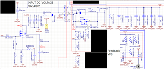
I need help with the implementation of a power supply using UCC38C40DR. It is a SMPS with a DC input voltage from 60V to 400 V and an output voltage equal to 12V/4A (UCC38C40 plus UCC24630) and 5V/1A (TPS 563208). My circuit schematic:
- Flyback topology:
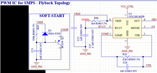
- UCC38C40:
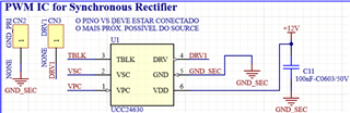
- UCC 24630:
My feedback voltage in pin 2 (VFB) is approximately constant and equal to 2.505V with load variations. The problem is the output voltage (load terminals) that significantly changes about 0.5 V with load variations (from no-load to about 40 W). This voltage fall may be because the resistor divider reads the output voltage in the VFB pin (R63 and R64), but this strategy is suggested in the datasheet, so it was not supposed to happen. I have this problem with load voltage regulation.
Any comments or suggestions are welcomed.
Thanks in advance.
