TIDA-01486: Is the DC offset in the receive paths necesasary since the receive path signal is AC coupled to the EVM430-FR6047

Part Number: TIDA-01486
Other Parts Discussed in Thread: TS5A3357, EVM430-FR6047, MSP430FR6047

Tool/software:

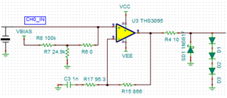
This is a section of the TIDA-01486 schematic that shows one of the 4 receive paths. There is a DC offset created at the input to the op amp. My question is this: Is this DC offset really necessary?
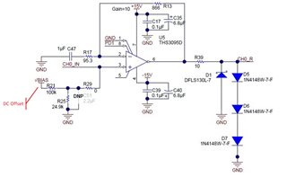
For the purpose of the TIDA-01486 design, I suppose the DC offset is necessary because, not shown in the schematic section pictured above, immediatly following the op amp output is the TS5A3357 switch which can only handle positive waveforms. And the switch is necessary so that the TIDA-01486 can support the switching for the 2 pairs of transducers.

But the output of the switch is AC coupled to the input of the EVM430FR6047 through a 1 nF capacitor (when using the TIDA-01486 with the EVM430-FR6047 evaluation board). If I wanted to create a design that incorporates this amplifier design for only 1 pair of transducers, then the DC offset ought not be becessary since it gets stripped away by that AC coupling capacitor.

Can you please confirm my thinking here?

  • Hi Anthony,

    According to the design guide of TIDA-01486, at the receiving signal, a 750-mV bias voltage is needed to cover the full range of the MSP430FR6047 MCU. You can get more design details from the design guide: https://www.ti.com/lit/ug/tidudo7/tidudo7.pdf. I think the need for DC bias depends on whether the amplifier output signal matches the back stage signal chain circuitry or the ADC sampling range.

    Best Regards,

    Yahui

  • Thanks for responding, Yahui.

    I have read the design guide and have gone over that section on page 4 where there is a single paragraph that says exactly what you said, that the bias voltage is needed to cover the full range of the MSP430FR6047.

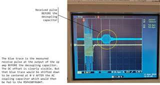
    But my main point is that the DC offset is removed by the AC coupling capacitor when the receive signal is fed to the MSP430FR6047. The following is a scope capture of a receive pulse that I measured. This pulse is BEFORE the AC coupling capacitor, but the blue trace would be shifted down to be centered at 0 V AFTER the AC coupling capacitor and then fed to the MSP430FR6047.

    However, the MSP430FR6047 can't handle the negative half od the pulse train, so I am confused about exactly what the MSP430FR6047 is seeing.

  • Hi Anthony,

    Could you please show the number of the AC coupling capacitor you mentioned and where it is located in the reference design. The signal before entering the MSP430 should theoretically not go through the AC coupling capacitor, that would lose the negative element of the signal.

    Best Regards,

    Yahui

  • Hello Yahui,

    The picture below is section of the MSP430-FR6047 evaluation board schematic (SLAR138B.PDF, page 2, section C5). This is where I have connected the TIDA-01486 signals to the MSP430-FR6047 evaulation board. The capactors C11 and C12 are both 1000 pF.

    I had to modifiy my evaluation board a little bit to separate the transmit signals from the receive signals. I was told by the author of the TIDA-01486 design that the amplified receive signals have to pass through the capacitors before they go to the MSP430 microcontroller. This next picture shows where I take the transmit signals from the evaluation board, and where I send the amplified received signals to the evaluation board.

    This is actually shown, although not explained very well, in the TIDA-01486 user guide, TIDUDO7.PDF. See either page 5 or page 6, the diagrams at the top. The right side of each of those diagrams shows capacitors in series with the receive pins of the MSP430.

    Are you saying that the capacitors shouldn't be used?

  • Hi Anthony,

    The circuit mainly amplifies the AC signal and after passing through the Schottky diode and the series silicon diode the signal level will be clamped at -0.3V to 1.8V.

    the input signal range of the MSP430 internal USS is also the same -0.3V to 1.8V, so MSP430 can handle it.

    Also the 1000pF capacitor you mentioned is needed for impedance matching, section 2.2.4 of the user guide has more details.

    Best Regards,

    Yahui

  • Yes, I am aware of the DC offset added to the received AC waveform, and I am aware of what those clamping diodes do. And I am aware of the need for impedance matching for the transmit and receive function for each transducer. But if you consider the receive signal, which is an AC signal of (in my particular case) a 1 MHz approximate sinewave superimposed on the 0.7 V DC offset. After the receive signal passes through the 1000 pF capacitor the DC offset is stripped away, right? Because the DC offset is purely DC and can't pass through the capacitor.

    Regardless of what I just said above, the circuit works and the MSP430 measures the receive signal. I'm just confused about how it works.

  • Hello Yahui;

    I read through those links you provided and I had originally connected my TIDA-01486 board to my EVM as per option #2 in ALEX OR's message. In this case, I was getting an overcurrent on the external +/- 15 V power supply so I thought that the DC offset from the receive path on the TIDA-01486 was causing a problem.

    But ALEX OR's option #2 causes more confusion. Let me explain...

    Let's say only the EVM430-FR6047 is being used, then the transducers are connected to J8 on the EVM. In this case, the transmit signal comes from the MSP430 and passes through either R16 or R17, depnding on which transducer is being fired. Then the receive signal from the other channel has to pass through the series capacitors C11 or C12, depending on which channel is receiving. Those capactors are guaranteeing that there is no DC offset on the receive signal. Remember, this is the EVM430-FR6047 evaluation board only.

    Now consider using the EVM430-FR6047 with the TIDA-01486 using ALEX OR's option #2 connection. In this case, the transmit signal go directly to the MUX's and then to the transmit path amplifiers on the TIDA-01486, and then out through either R35, R36, R37, or R38 on J4 on the TIDA-01486 to one of the transducers. The corresponding receive signal from the other channel has to pass through a series capacitor either C23, C24, C25, or C26, depending on which transducer received the signal. That capacitor guarantees there is no DC offset on the receive signal at this point. Then the receive signal passes through the receive path amplifier where a DC offset is added to the AC signal, then passes through the receive path MUX, and if ALEX OR's option #2 connection is used to connect the TIDA-01486 to the EVM430-FR4067, there is an AC receive burst signal superimposed on the a DC offset. You can follow the signal through the TIDA-01486 schematic, so I won't repeat it here.

    My point is that in the first case I described which is just the EVM430-FR6047 only, there is no DC offset on the receive signal. In the second case which is the EVM430-FR6047 used with the TIDA-01486, there is an AC burst signal superimposed on a DC offset. These two cases are different.

    So you can see my confusion. I'm still not 100% sure how to connect the TIDA-01486 to the EVM430-FR6047.

  • Hi Anthony,

    If you are using a pair of sensors you can leave out the multiplexer. And in the second case, make sure that when J3 on the TIDA connected to J8 on the 430EVM board, the R and C for the same pair of inputs and outputs on J8 should not connected together.

    please try this link: https://e2e.ti.com/support/microcontrollers/msp-low-power-microcontrollers-group/msp430/f/msp-low-power-microcontroller-forum/904956/evm430-fr6047-one-ultrasonic-pair-connexion-between-tida-0486-and-the-evm

    thanks,

    Yahui