This thread has been locked.

If you have a related question, please click the "Ask a related question" button in the top right corner. The newly created question will be automatically linked to this question.

TINA/Spice/LMH6521: Distinction between Spice model and simulation curve in datasheet

Part Number: LMH6521
Other Parts Discussed in Thread: TINA-TI,

Tool/software: TINA-TI or Spice Models

I noticed a few distinctions where the simulation result of the spice model in ADS does not meet the curves in the datasheet.

I would like to get clarified which one is more close to reality.

If it is the model that is inaccurate, my major concern is maybe I make wrong design choice when running simulation with the model in the design phase.

I would first like to get the doubts clarified and would appreciate it if the model can get closer to reality. 

The model in this test is LMH6521. The datasheet I am referring is version: SNOSB47E –MAY 2011–REVISED AUGUST 2016

Below are the distinctions observed:

1. S11 versus attenuation setting:

 It would seem that the input attenuator of the device is a passive network. If this is true, S11, i.e. reflection, should get better with increased attenuator setting. However, this is not what is observed in the model.

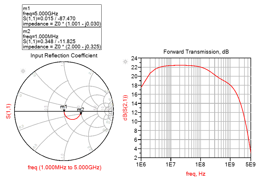
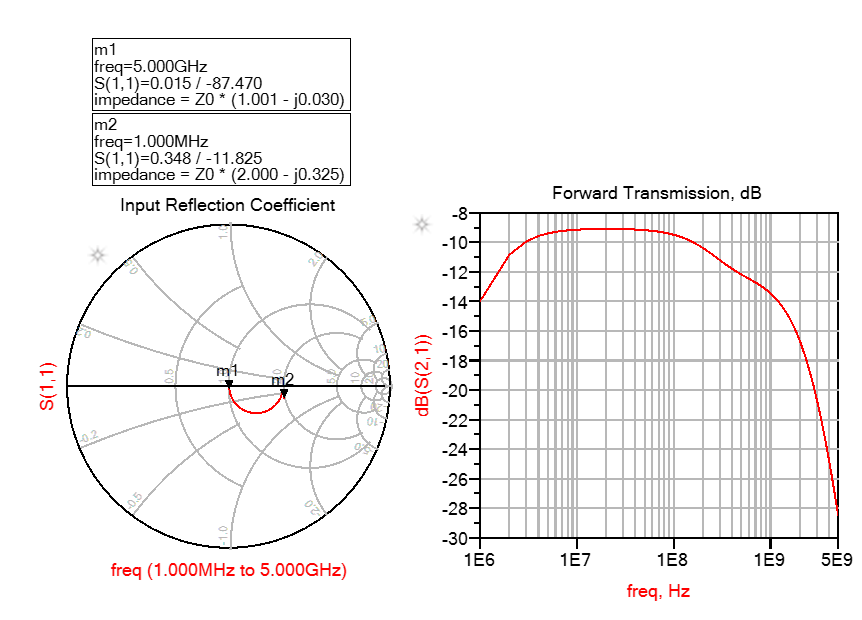
ADS simulation curves with the spice model:

S11 at MAX gain setting, together with S21

S11 at MIN gain setting, together with S21


The change of gain setting is observable from S21. In the two situation, S11 makes no difference, i.e. smaller reflection is not observed at higher attenuation setting. This raises the question whether the input impedance is properly modeled.

2. Large distinction in gain curve at low gain setting

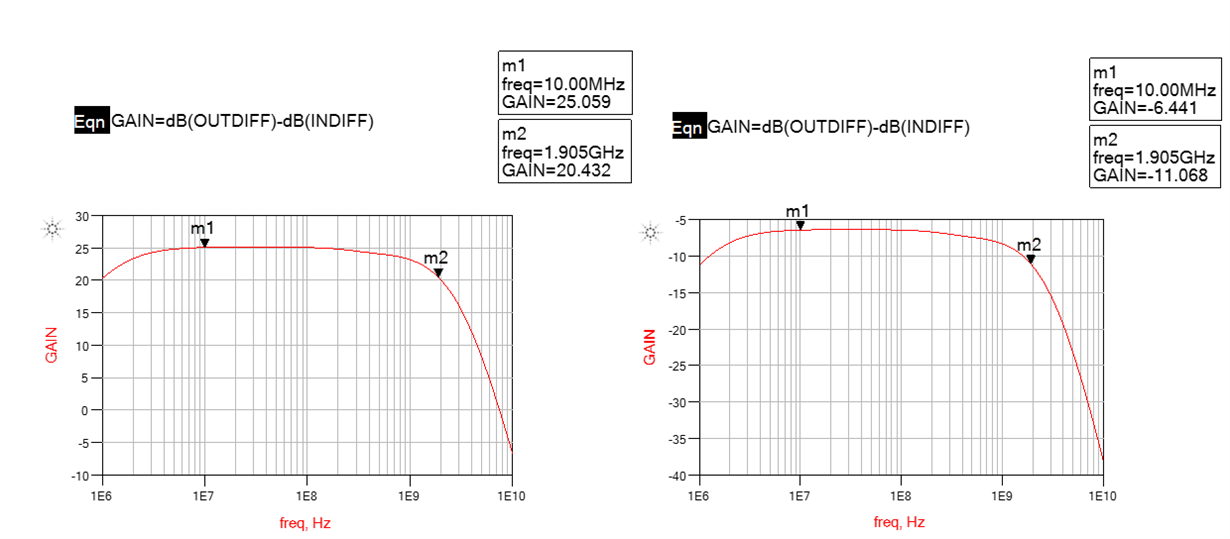
Below are the simulation gain curves at MAX and MIN gain settings. As can be seen, the curve has the same shape in either cases. 

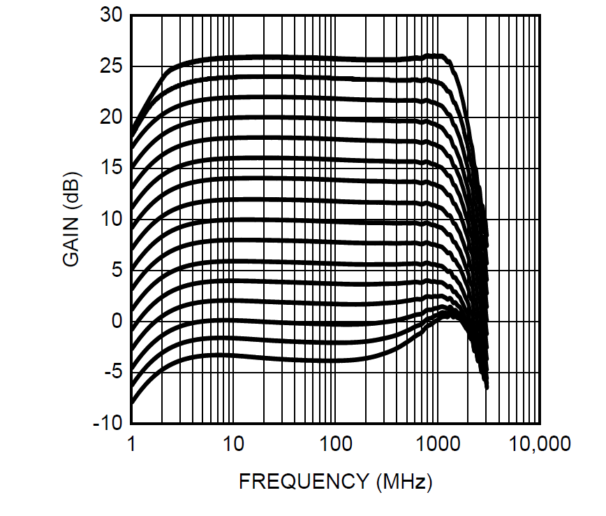
Meanwhile, below is the gain curves versus attenuation setting in the datasheet. There is clearly a peak just before the gain drops, which becomes more obvious in low gain settings. Although it is not a direct interest to know the gain curve in the settings that gain is smaller than 0 dB. I think this phenomenon underlies that the model missed a few poles and zeroes in the frequency of interest compared to the device. I would like to get a bit more clarification on that, such as whether they are internal or at the output stage and then assess the impact on the design.

  • Yuan,
    A couple of approximations were made during the design of this model.

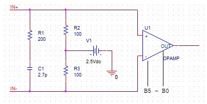
    First, the attenuator was approximated as a gain/loss block that is controlled by the control bits. The attenuator's input impedance is implemented at the analog input pins. A simplified schematic is shown below.That is why the input impedance does not change as the attenuator is adjusted.

    Second, the gain block frequency response does not change with attenuator settings. The gain block is modeled as a flat gain with some voltage limiting, followed by three first-order 3.2GHz low-pass filters. This and the first item combine to keep the frequency response shape unchanged as the attenuator is adjusted.

    I hope this helps.
    Please let me know if you have any more questions.

    Regards,
    John

  • Sorry Yuan.

    I forgot to attach the diagram of the input circuit  before posting.

    It appears below

     .

    Regards,
    John

  • Hi John,

    If I understand correctly, the input impedance is not a calculation of the RC in parallel with the amplifier input impedance, but rather a value overwritten by some value provided by 'pin'?
  • Yuan,
    Sorry I wasn't clear.
    In the model, the model's input impedance is controlled by the R's and C's attached to model's input pins.

    In contrast, the real device the input impedance results from some parasitic and internal components at the input pins, as well as components making up the attenuator. For low attenuator settings, the input impedance of the internal gain amp probably contributes as well.

    The model approximates this more complex network via the diagram in my last message.
    Regards,
    John
  • Hi John,

    Thanks for the explanation.

    So, the input impedance is set by the RC network in the following figure, the triangular-amplifier has some infinite input impedance and the variable gain is reflected in the model by changing some virtual variable, which does not lead to a change in input impedance of the triangular-amplifier?

  • Yuan,
    I forgot to add some notation in that figure. The triangular shape represents the attenuator, and it does have an infinite input impedance. So even as the attenuator settings change by varying {B5,...,B0}, the input impedance of the model is still set by R1-R3 and C1.
    Regards,
    John
  • John,

    Thanks for the clarification. I understand now the behavior of the input impedance in the simulation.

    Based on this, may I say that the information regarding input impedance at different gain setting is missing? Is there any more information regarding this?

    Regards.
  • Yuan,
    You are right. The info on input impedance versus gain settings is missing from the datasheet.
    I do not have any additional info on this, but I will check with the group responsible for the device.
    I will reply to this thread once I have any answer. It will probably be a few days.
    Regards,
    John
  • Hello Yuan,

    I will try to answer some of your questions:

    1.  The input attenuator does not change very much with gain changes.    The gain is changed by selecting which node of the input attenuator is active. This means that when the gain changes the observed input impedance has very little change. 

    2.  Likewise the output amplifier is always set to maximum gain, so the output impedance is very consistent over gain settings.

    3.  The datasheet curves were based on measurements done on the evaluation board.  We did our best to de-embed the PCB parasitics, but the curves are still not completely accurate with respect to the device input pins. 

    4.  The peaking you see at low frequencies is not actual peaking.  It is actually signal feed through that basically bypasses the attenuator stage.  You can imagine that it is due to very small capacitors in parallel with the input attenuator stages.    Further, this behavior is not absent at higher gains,it is only being masked by the stronger signal path that exists at higher gains. 

    5.  I have had best results treating the LMH6521 as a purely resistive 200 Ohm load when designing filters. 

    Regards,

    Loren

  • Hi Loren,

    Thanks for the explanation. I would appreciate if you can further attend to the following questions marked in green

    1.  The input attenuator does not change very much with gain changes.    The gain is changed by selecting which node of the input attenuator is active. This means that when the gain changes the observed input impedance has very little change. 

    Would it be close if I understand it in the way that the input of LMH6521 is a resistor ladder and the 1st amplification stage is connected in parallel with the resistor ladder. In this way, both the attenuation and attenuation-insensitive input impedance can be explained.

    2.  Likewise the output amplifier is always set to maximum gain, so the output impedance is very consistent over gain settings.

    Okay. This is clear.

    3.  The datasheet curves were based on measurements done on the evaluation board.  We did our best to de-embed the PCB parasitics, but the curves are still not completely accurate with respect to the device input pins. 

    Okay. This is clear.

    4.  The peaking you see at low frequencies is not actual peaking.  It is actually signal feed through that basically bypasses the attenuator stage.  You can imagine that it is due to very small capacitors in parallel with the input attenuator stages.    Further, this behavior is not absent at higher gains,it is only being masked by the stronger signal path that exists at higher gains. 

    Okay. This is clear.

    5.  I have had best results treating the LMH6521 as a purely resistive 200 Ohm load when designing filters.

    Even when given the fact that the datasheet shows frequency-sensitive input impedance, which is 200 Ohm at DC and reduces to 100 Ohm at 500 MHz? Do you expect this reduction at high frequency mainly due to the remaining parasitics during measurement? What can you say about the impedance above 500 MHz? What would be the recommendation if LMH6521 is planned to be used up to 1 GHz and following a 100-Ohm LPF?

  • Hello Yuan,

    #1. Would it be close if I understand it in the way that the input of LMH6521 is a resistor ladder and the 1st amplification stage is connected in parallel with the resistor ladder. In this way, both the attenuation and attenuation-insensitive input impedance can be explained.

    Yes, the input is a resistor ladder attenuator.

    #2. Even when given the fact that the datasheet shows frequency-sensitive input impedance, which is 200 Ohm at DC and reduces to 100 Ohm at 500 MHz?

    Some of this impedance change is due to the EVM. The actual amplifier is still very close to 200Ohms at 500 MHz.

    #3 What can you say about the impedance above 500 MHz? The impedance will gradually decrease with increasing frequency. It will be a single pole roll off due to the input capacitance of the amplifier and the capacitance of the PCB traces next to the amplifier. Your board design will determine the exact behavior.

    #4 What would be the recommendation if LMH6521 is planned to be used up to 1 GHz and following a 100-Ohm LPF?

    I would recommend placing a 200 Ohm resistor in parallel with the amplifier input to match it to 100 Ohms. There is a chance that you could improve the performance by using a resistor in series with an inductor such that at higher frequencies the total impedance is still 100 Ohms, but I am not 100% confident this will be successful. One reason is that inductors are physically large and the extra room that the inductor takes up in the layout is harmful to circuit performance. Another reason is that many inductors are capativice at 1GHz which is also harmful to circuit performance. If you have time and resources to test this idea it would be good to try, but if not then just use the resistor. You can still experiment with the resistor value. For example, using a 220 Ohm resistor would still match well at lower frequency, but would give more frequency range where the total impedance is close to 100 Ohms.

    Overall, I would recommend making as good a match as you can for frequencies up to 500MHz, and then let the higher frequencies do what they will. You will get the most benefit by making sure that the filter is less than 1cm away from the LMH6521 input pins. When the interconnect traces are very short then the matching between the amplifier and the filter is much less important. One benefit of low pass filters is that they are pretty forgiving of impedance mis match.


    I have one more thing to add. When you design your 100 Ohm low pass filter it may be good to design it for about 5% to 10% higher frequency. It seems that every filter I design has a lower frequency response when I build it on a PC board. I have started designing my filters for a slightly higher frequency than desired and it reduces the time it takes to tune the filter when I build my prototype. Maybe you are already expert in this area and don't need my input, but this method has helped me in the past.

    Regards,
    Loren