This thread has been locked.

If you have a related question, please click the "Ask a related question" button in the top right corner. The newly created question will be automatically linked to this question.

TIDA-00951: TIDA-00951 Schematic/PCB not match with BOM.

Part Number: TIDA-00951

Hi everyone, 

- We are involved in the manufacturing of this TIDA-00951 Starter kit. We have sent the PCBs design to the manufacturer and they have sent back to us the PCBs already built. OK

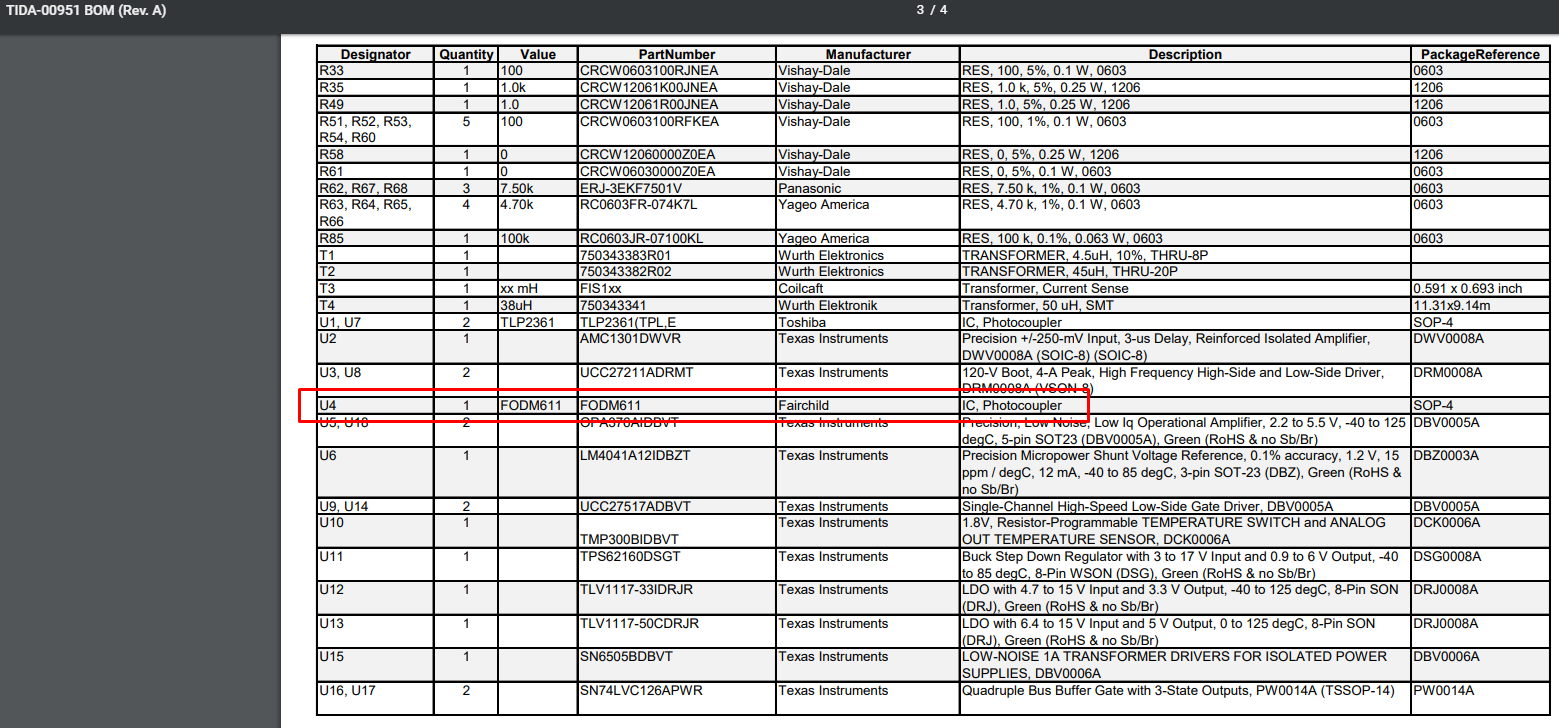
- In parallel, we have bought all the components of the BOM showed in the TIDA 00951 Technical files. OK.

Then, when we are soldering these BOM devices on the manufactured PCB, we have noted that, the component U4 (Optocoupler) has not the same footprint and definetly, the component in the BOM is another different (5 pins and another internal schematic) respected to the Altium PCB/schematic, which is an optocoupler of 4 pins and different internal schematic.

Until this moment, we have note only that this component does not match between Altium Schematic/PCB and BOM. But we are not sure about the others of the BOM auntil we solder them in the following days.

We think that this issue needs to be revised by TI.

Thanks,

Guillermo Perez, R&D Power Electronics Engineer from University of Seville, Spain

  • HI,

    Please use the 4 pin LTV-817. We updated the schematic online sometine back but looks like the BOM is not showing the latest version. I will update it shortlly.

    Best Regards,

    Ram

  • Dear Ram,

    Ok, I hope you can modify the BOM showed with the final Schematic components. The strange thing is that the BOM modification date is newer compared with the Schematic file...

    We are in touch.

    Best regards,

    Guillermo
  • Dear Ram,

    We have noticed some extra components that don't match between Altium and BOM:

    1) C12: in the BOM appears with one description which is incorrect because the footprint used in Altium is for a 100pF 0603 capacitor, not for a thru-hole one. Solution: Update the BOM with the 100pF unit (same model as C40).

    2) R47: in Altium, the component part number (0603) does not match with the used footprint (1206). Solution:  You need to update the component in Altium to use 0603 footprint showed in the BOM.

    3) C15, C25: in Altium, the component part number (0603) does not match with the used footprint (1206). Solution:  You need to update the component in Altium to use 0603 footprint showed in the BOM.

    Regards,

    Guillermo Perez

  • Hi Guillermo,

    Thanks for bringing these to our notice. Your help in improving the quality of out TI Design documentation is greatly appreciated. We will get these changes done as soon as possible.

    Regards,

    Salil
  • Hi Salil,

    Ok, thank you for your words. Here are some extra components to modify in your design:

    - D16, D17 -> The footprint used is not suitable for the diameter of his legs. The hole is too small and the MBR3100 component can not be inserted in his footprint. Solution: change the footprint holes to another at least 10mils bigger.

    - HS1, HS2 -> The component shown in the BOM is not same used in Altium, so footprint does not match with the component shown in the BOM. Solution, change the component in the BOM by the right one.

    Regards,

    Guillermo

  • Hi,

    Another component to modify:

    - J9, J10, J11 and J12: You use a footprint in Altium that has exactly the same diameter (1.47mm) that Wurth specifies in his datasheet for these part number (1.475mm). So in the real PCB, the component doesn't fix in the holes, due probably to manufacturing tolerances or whatever. Solution: Increase the hole sizes in the footprint for these components.


    Regards,

    Guillermo
  • Hi Guillermo,

    We are in the process of updating the TID incorporating the suggestions provided by you. Thank you once again.

    Regards,

    Salil
  • Hi TI,

    We are having problems with the reading of the ADC channel whta comes from the VBUS voltage level. And we have found two different versions of the accomodation signal circuit from VBUS point to the ADC B6 channel. The question is, what is the correct between these two schematics?

    1) Circuit shown on the PDF of the TIDA-00951 section 6.3.1.7 Isolated Voltage Sensing: http://www.ti.com/lit/ug/tidud04/tidud04.pdf 

    2) Circuit shown on the SCHEMATIC of the TIDA-00951 Sheet 3, and for that, the final ALTIUM project and physical PCB: http://www.ti.com/lit/df/tidrr65/tidrr65.pdf 

    We are reading always in Code Composer the same value in bits (Saturation): 4095 no matters the voltage in the pin VBUS of the power circuit, so please. Let us know what circuit of the shown above is the correct.

    Have a nice day,

    Guillermo Perez

  • Good morning TI,

    Regarding the last issue about the VBUs signal conditioning with the AMC1301 and the OPA276 circuit, both versions (TIDA-00951 and Altium files from your product website) are wrong.

    We have simulated both versions of the circuit in LTSpice and none of them works as espected, so we have searching on different application notes related to the AMC1301 and OPA376 as an isolated signal conditioning and we have found the right configuration, which works fine in LTSpice. This circuit is shown below:

    - We have simulated with good results this circuit so, the question is, What do you think about this? What is the solution?

    Thanks,

    Guillermo Perez

  •  Hi Guillermo ,

    Please use the schematic snippet attached with this mail. I will send you an email with the DNP parts toady.

    Best Regards,

    Ram

  • Hi, I have post a new Post related to Hardware, to discuss about these issues/modifications, not related with the Altium vs. BOM missmatching: e2e.ti.com/.../2756865
  • Dear Ram,

    The circuit you proposed for the VBUS sensing saturates its output too early, I  have simulated your proposal. See the attached picture:

    We have implemented this circuit and it shows better response both in simulation and in real Hardware testing:

    What do you think?

    Thank you

  • Hi Guillermo,

    The R7 and C3 need to connected to the +ve input terminal of the opamp in the first simulation that you showed.

    Adding a 1.2V offset in the 2nd simualtion is not a problem as such. It will result in an ADC ofset of +1.2V at 0 input voltage on the BUS.

    In the cirucit 1 simulated with the changes I suggested in this post, you should be able to elimiante the offset. The TIDA-00951 firmware will expect close to 0V offset at 0V Bus input, unless you change it accept a 1.2V offset.

    Best Regards,

    Ram