This thread has been locked.
If you have a related question, please click the "Ask a related question" button in the top right corner. The newly created question will be automatically linked to this question.
Tool/software: WEBENCH® Design Tools
Dear Ti Forum,
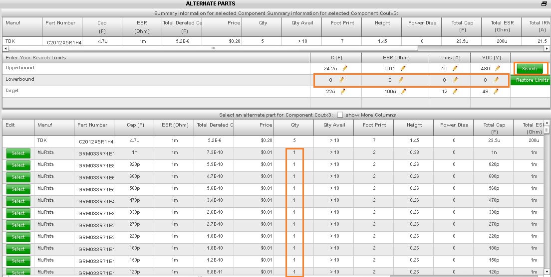
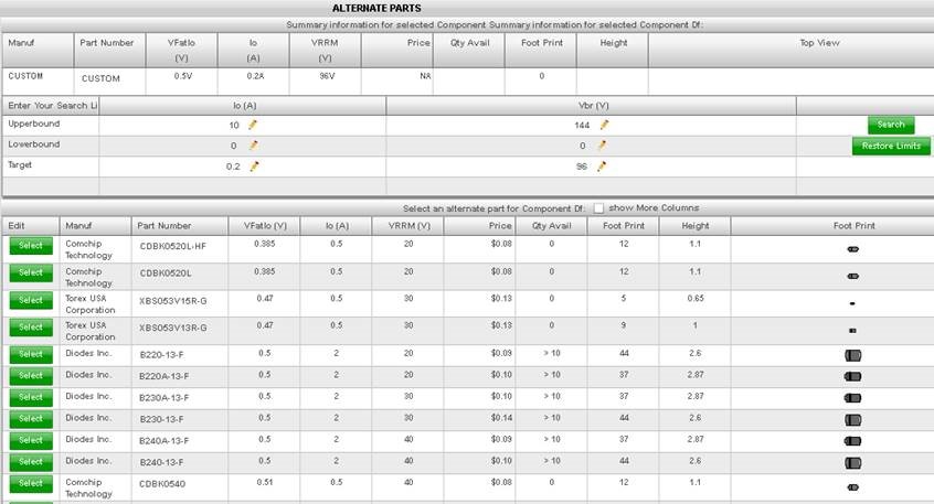
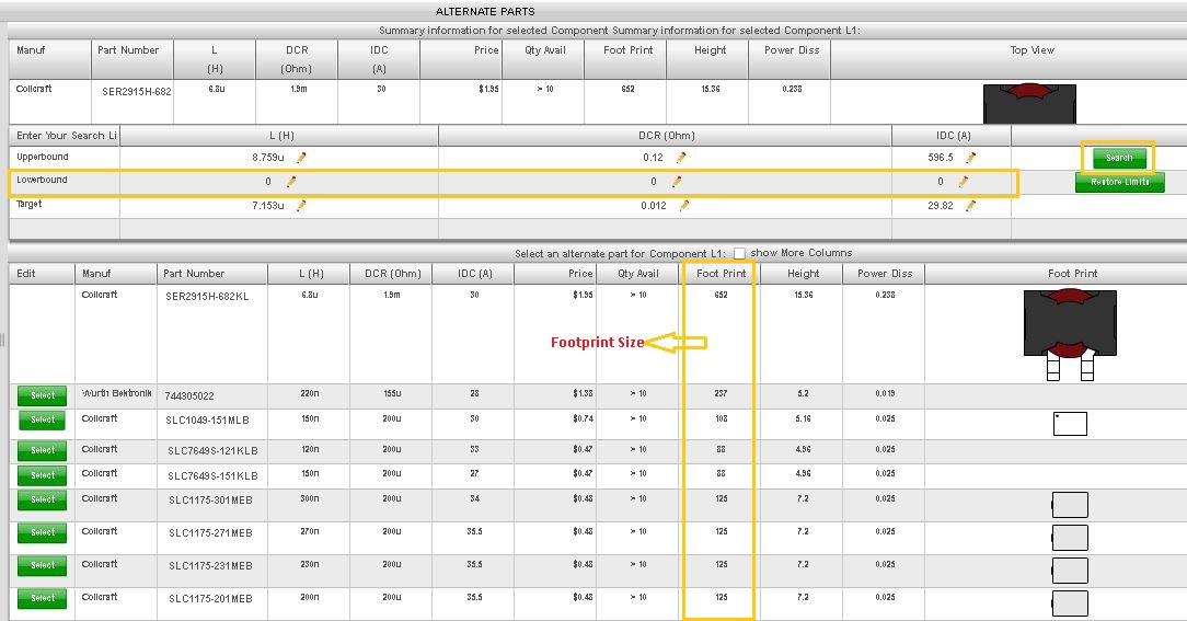
I Have created a Workbench Design for DC to DC charger using LM5176 variable Input 12-48V and Fix O/p 24V @ 10A for charging the battery. My design link is "webench.ti.com/.../SDP.cgi. Now my questions are
1.> "can i use it directly? "
2.> "When i try to download CAD export for PCB layout using 'Altium Designer' I keep getting error as 'L1 is too Big to Fit Horizontally!', but i can still download the PCBdoc file. as soon as i download it i see it is jumbled PCB layout. Can you tell me what is wrong? Is there some altium designer version specific i need to open on? I'm using Altium Designer S09v.
Deeply awaiting your reply.
Hi Vijay,
Thanks for choosing WEBENCH.
We are working on your query and will get back to you shortly.
Thanks and Regards,
S.Suganya
Hi Vijay,
With reference to your design conditions(Inputs 12V to 48V and Fixed Output 24V @ 10A) we observe component Overlaps and footprint missing. Please follow the below steps to rectify the same.
1. Coutx, Coutx2 and Coutx3 are more than 1 quantity as per design conditions and hence they are overlapping.
Single quantity capacitors with required capacitance as per design your design requirements can be selected from the ‘Alternate list’ by making the Lower bound as ‘zero’ and modifying the ‘Upper bound’ and ‘Target’ as shown in the below image.
2. Dboot1 is fetching a 3 pin diode as per the design requirements. Alternate 2 pin diode could be selected in a similar way above. SMA or SMB footprint with required Inductance value would fit better in the given PCB area.
3. Df is appearing as a ‘CUSTOM’ component and hence it is missing in the PCB. CUSTOM components are not supported in CAD exports. Please select a part number for Df in the Alternate component list by modifying the bounds as shown below.
4. Ccomp capacitor is bigger(1812 package) and overlapping the nearby traces as per the design requirements. Please choose 0805 package size capacitor with required capacitance value from the Alternate list.
5. L1 is fetching a 3 pin Inductor as per the design requirements and it is bigger in size than the given area. 3 pin Inductors are usually not supported by WEBENCH exports. Please choose a comparatively smaller size Inductor preferably a footprint size which is less than or equal to 339 from the ‘Alternate List’ with the required Inductance that matches your design requirements as shown below.
Please Note:
a. While searching for Alternate components try making ‘Lower Bound’ as ‘zero’ which fetches many part numbers in the result.
b. Always choose a part number that actually matches your design requirements from the Alternate List.
c. Once the above steps are done, Repour copper polygons to refresh the PCB design.
In reply for question 1,
Please use the Schematic and PCB after the above modifications for Simulation purposes.
Thanks and Regards,
S.Suganya
Hi,
I Appreciate your detailed reply.. Iw ill check accordingly. Thank you again!