This thread has been locked.

If you have a related question, please click the "Ask a related question" button in the top right corner. The newly created question will be automatically linked to this question.

TIDA-00778: change IGBT to NMOSFETs in parallel

Part Number: TIDA-00778
Other Parts Discussed in Thread: UCC27714, TIDA-00364, UCC27211, TIDA-00472, UCC27712-Q1

Dear TI Experts:

I have a targeted application (rated 3KW, Vbus=86V for a 3 phase PMSM control ). I found TIDA-00778 is a powerful design.

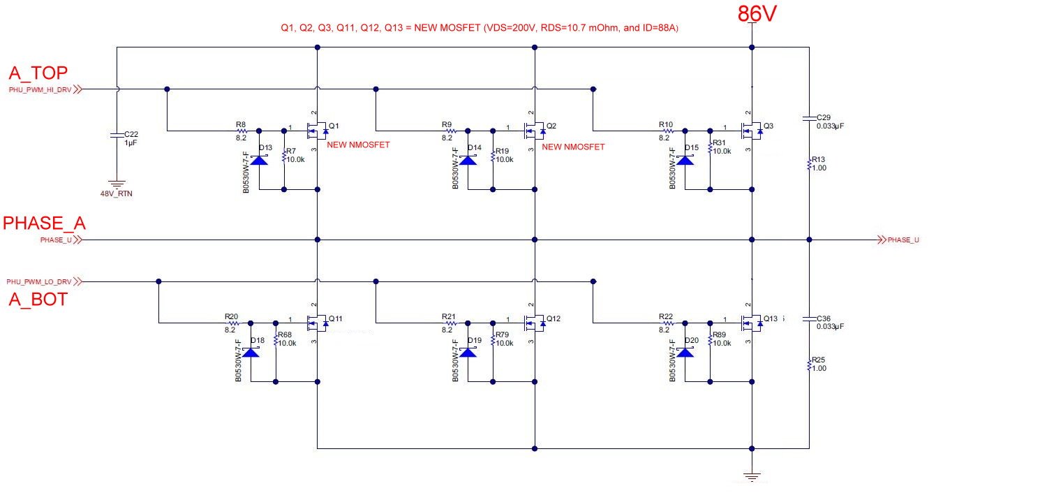
Now I hope to apply the following UCC27714 gate driver design to drive NMOSFETs, instead of a IGBT. 

The spec. of the NMOSFET I found is VDS=200V, RDS=10.7 mOhm, and ID=88A.  Also, I will apply parallel operation of power MOSFETs (I will arrange 3 NMOSFETs in parallel. It is 5 FETs in parallel in TIDA-00364)

Since UCC27714 is much more powerful than UCC27211 (in TIDA-00364), is it feasible to apply the following gate driver design to drive NMOSFETs in parallel?

Could you kindly reply me?

Wish you the best!

Tang Han

  • Hi Tang,

    The UCC27714 and UCC27211 has similar source and sink peak current rating. However with 86V DC bus voltage, if we consider the voltage tolerance and switching spikes, the design margin may be low with the 120V driver. The UCC27714 could be used for such application.

    The circuit snap shot (figure 20) above from TIDA-00778, is the design for driving a single IGBT/MOSFET. When you parallel the MOSFETs, you need to ensure that each FET is connected to the gate driver output through separate sink/source gate resistor. I would recommend to refer TIDA-00364 schematic for the same. Use a similar circuit from TIDA-00364 at the output of UCC27714.

    In short, the gate drive output stage circuit of UCC27211 in TIDA-00364 can be referred to design the output stage circuit of UCC27714 when you parallel the MOSFETs.

    Please let me know if you have any question.

    Thanks & Best Regards,

    Manu

  • Dear Manu:

    I am so grateful to you for your kind, experienced, and professional reply.
    Your every word is so valuable for me!
    In order not to mistake what you guide, I draw the following diagram (one phase), where A_TOP, PHASE_A, and A_BOT are the outputs of the previous UCC27714 gate driver circuit. Could you kindly check it for me?
    1. Are the values of gate resistors R8-R10 and R20-R22 suitable?
    2. Are the zener diodes D13-D15 and D18-D20 suitable?  Are the R7, R19, R31, R68, R79, and R89 suitable?  I have bought a DRV-8301-HC-C2-KIT, but where it seems no such protection circuits for MOSFETs. Of course, the protection circuits are good. Could you check it for me? Now I have changed the NMOSFETs to VDS=200V, RDS=10.7mOhm, and ID=88A.

    3. In the TIDA-00364 design, there are added pnp BJTs (MJD45H11RLG) at the end of Gate Driver circuit, as shown in Figure 4 (Page 6) of TIDA-00364 document. Is the added circuit necessary? Or can be omitted since UCC27714 is much more powerful than UCC27211? 

    Look forward to hearing from you~

    I appreciate your kind help so much!

    Wish you a prosperous new year!

    Tang Han

  • Hi Tang Han,

    Please find below my suggestions to your questions.

    1. You may need to adjust the gate resistor values according to the MOSFETs used and PCB parasitics to optimize the switching performance. Start your design with 8.2 ohm and during testing tune this value to get an optimized clean FET switching waveforms.

    2. The existing diodes (D13-D15 and D18-D20) and resistors (R7, R19, R31, R68, R79, and R89) should work.

    3. The pnp BJTs are added to enable a strong pull down during MOSFET turn off as the gate path length is more in TIDA-00364(due to 5 FETs in parallel). However in your case, since you are paralleling only 3 FETs, the board can be compact and if the gate drive path from the gate driver to FETs are small, the BJTs can be avoided. This depends on the PCB layout. One recommendation could be, keep provision in the prototype design and during testing check whether you need the BJT or not to get an optimum FET switching. Refer TIDA-00364 for more details.

    Thanks & Regards,

    Manu

  • Dear Manu:

    How pleased I am to hear from you!   ^_^
    Thanks for your confirmation of the above circuit, which I can start from.   I will also add diodes (D13-D15 and D18-D20) and resistors (R7, R19, R31, R68, R79, and R89) to protect the MOSFETS.
    I find UCC27714 is much more complicated than UCC27211. I don't know how to add the BJTs. I hope that as you said, "the BJTs may be avoided".   ^_^

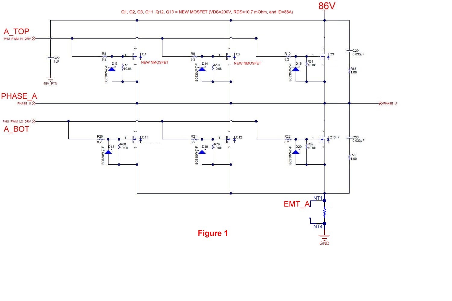
    1. For the following one phase circuit, I have added the Rshunt to sense phase current for PMSM FOC control.  In this manner, The 'NT1', one end of Rshunt, should connect to 'EMT_A', the 'COM' pin of UCC27714, right?  

    2. Could you also kindly check C29, R13, C36, and R25 (on the far right ) for me?  (One end of R25 is connected to NT1, instead of GND, right?)  

    3. Based on the following circuit, I can continue to add a voltage divider circuit for sensing the voltage of PHASE_A for PMSM FOC control, right?   If I want to sense the Vbus voltage (86V), I can continue to add a voltage divider circuit for sensing the voltage of Vbus, right?  Will these circuits influence the snubber function  of C29, R13, C36, and R25 (on the far right )?  ^_^

    I am sorry to ask these stupid questions. Look forward to receiving your kind and professional reply~

    Wish you the best!

    Tang Han

  • Hi Tang Han,

    Let me add a comment on " the BJTs may be avoided". You should make sure that the the gate return path length from the MOSFETs to the gate driver should be very short. Further to your questions. I see you are planning for single shunt FOC, right?

    1. Yes, NT1 should be connected to the COM pin of UCC27714. Make sure that you use a bypass capacitor between VDD and COM as recommended by datasheet. You can refer TIDA-00778 schematic

    2. The connection of snubber to NT1 is debatable. However the capacitance value is 33nF, which is low and connection to NT1 should be ok.

    3. You can add the voltage divider for the PHASE nodes and Vbus terminal. I don't see a problem to the snubber with the voltage dividers.

    Regards,
    Manu
  • Dear Manu:

    You are such an experienced and professional expert I have ever seen.  ^_^  Thanks for your kindness to me~

    My targeted application is a 3 phase PMSM control (rated 3KW, peak 7.2 KW, Vbus=86V). I will apply 3-shunt  FOC control. For the above Figure, only one phase is shown.  The left two phases will be the same as the one I showed. Is it OK?

    1. The NMOSFET I originally chose is VDS=200V, RDS=10.7 mOhm, and ID=88A.

       Recently I have found a new NMOSFET with VDS=150V, RDS=4.4 mOhm, and ID=174A. Could you kindly give me suggestion that which one is more suitable for my application?    ^_^

    2. From the BOM table of TIDA-00364 provided by TI, I found the spec. of gate resistors, R8-R10 and R20-R22, are  "RES, 8.2, 5%, 0.125 W".

        Since the Vbus=48V in TIDA-00364, but now my Vbus=86V.  Do I need to increase the spec. of 'Power =0.125 W' to a higher voltage?

    3.  From the BOM table of TIDA-00364 provided by TI, I found the spec. of D13-D15 and D18-D20 (around the MOSFETs) is  "Diode, Schottky, 30 V, 0.5 A".  

        Since the Vbus=48V in TIDA-00364, but now my Vbus=86V.  Do I need to increase the spec. of 'reverse voltage =30V and forward current=0.5A' to a higher voltage?

    4. From the BOM table of TIDA-00364 provided by TI, I found the spec. of R7, R19, R31, R68, R79, R89 (around the MOSFETs) is  "RES, 10.0 k, 1%, 0.1 W".  

        Since the Vbus=48V in TIDA-00364, but now my Vbus=86V.  Do I need to increase the spec. of  'Power=0.1W' to a higher voltage?

    5. From the BOM table of TIDA-00364 provided by TI, I found the spec. of R13 and R25 (RC snubber on the far right) is  "RES, 1.00, 1%, 1 W, AEC-Q200 Grade 0".

        Since the Vbus=48V in TIDA-00364, but now my Vbus=86V.  Do I need to increase the spec. of 'Power=1 W' to a higher voltage?

    I am so sorry to bother you so much.  The above may be the last questions. Look forward to hearing from you~

    Wish you the best!

    Tang Han

  • Hi Tang Han,

    Please find my responses below.

    1. I would go for the lowest RDS device, provided, the design should make sure that the voltage spikes across FETs  should be limited well below the maximum VDS of the device. You need to tune the gate circuit resistor to slow down the FET switching to limit the voltage spikes across the FETs during switching. You can consider adding snubber on the switching nodes (phase outputs) also.

    2. Calculate the average gate resistor power loss based on the Qg of the MOSFET, switching frequency and VGS. Note that your gate circuit voltage is around 12V only (independent of Vbus =48 or 86V)

    3. You can use the same D13-D15 and D18-D20 (Diode chottky, 30 V, 0.5 A"), as these diodes are connected across gate and source, they will be working at VGS voltage not at the Vbus voltage

    4. No need to increase the power rating of R7, R19, R31, R68, R79, R89  (reason same as above point 3)

    5. You have to calculate the snubber resistor loss. Please refer any standard document and calculate the snubber loss at 86V.  You may have to increase the power rating. The average power loss depends on the Vbus, switching frequency etc.

    Thanks & Regards,

    Manu

  • Dear Manu:

    You have taught me a lot again. I am so grateful to you~  

    Q1:  You mentioned, "Note that your gate circuit voltage is around 12V only (independent of Vbus =48 or 86V)".  Does the "gate circuit voltage 12V" mean the VGS?   But if YES, I found the VGS value may be different for each NMOSFET. So, I am a little confused.

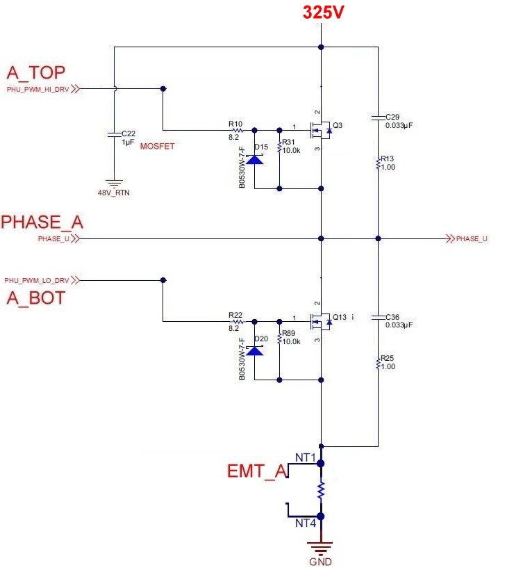
    I have another targeted application on a 3-phase PMSM FOC control (230VAC input, Vbus ~= 325V, 420W)

    I will also reference the TIDA-00778, and use UCC27714 as the gate driver.  I have found NMOSFETs with VDS=800V, RDS=1.55 Ohm, ID=8A, and @VGS=10V.

    Since the rated power is only 420W, so MOSFETs are not needed to be in parallel this time, right?

    I have plotted the one-phase circuit as follows, and hope that you can kindly check it for me. 

    Q2: In the following circuit, Q3 and Q13 are NMOSFETs with VDS=800V, RDS=1.55 Ohm, ID=8A, and @VGS=10V.

    For these components, such as C22, D15, D20, R31, R89, C29, C36, R13, and R25, are they also required to make the system more stable?

    Look forward to hearing from you~

    Many thanks to you!

    Tang Han

  • Hi Tang,

    The gate driver VDD determines the gate circuit voltage. Typically the MOSFETs are rated for maximum VGS of 20V. So we typically uses 10V/12V/15V supplies with the gate driver to ensure the minimum RDS operation of the MOSFETs. In this case if the UCC27714 uses 12V power supply, then the gate circuit voltage will be 12V.

    For your design with 230V AC input, I would suggest you to refer the TI designs, TIDA-00472, and TIDA-00778 and use the similar circuit topology. You can still uses the diodes and resistors (D15, D20, R31, R89...) across gate and source of the MOSFET.

    There is no need to parallel the FETs for 420W. You may be able to use a 600V FET with even lower RDS to reduce the power loss in FETs.

    I would suggest you to study the datasheet of UCC27714 and the TI design document to understand clear and deep about the circuit design.

    Thanks,

    Manu

  • Dear Manu :

    You are right!  I should study more from datasheet and TI documents.   ^_^

    But now I have an urgent question. Could you kindly reply me?   In TIDA-00778, the UCC27714 uses 15V gate circuit voltage as shown below. (In TIDA-00364, the UCC27211 uses 12V gate circuit voltage )

    In the following circuit, if we directly replace the power supply from 15V to 12V, we should adjust certain values of R and C in the circuit, right?   

    Thanks for introducing  TIDA-00472 and TIDA-00778 , I will carefully learn their design.

    Wish you the best!

    Tang Han

  • Hi Tang,

    Yes, you are right. You have to tune the resistor values when you change the supply from 15V to 12V. Also, as discussed previously, you have tune the gate resistors based on the MOSFET you have used. Please refer the TI designs TIDA-00472 or TIDA-00778 or the datasheet of UCC27714 for design calculations.

    Regards,

    Manu

  • Dear Manu:

    1. I am sorry that I hope to find an AEC-Q100 Qualified gate drive to replace UCC27714. Could you kindly suggest a suitable one? 

    I only find a similar one UCC27712-Q1 with smaller sink and source current than UCC27714.  Do you think it is a good one for my targeted application (Vbus=86V rated 3KW) (3 MOSFETs in parallel as I previouly mentioned)?

    2. For UCC27712-Q1, I found its circuit, provided by datasheet (shown below) is so simple.  I can't even find the gate resistor.  Is it due to AEC-Q100 Qualified? So it is more powerful?  Or in fact, the circuit can't be so simple!  Is there any practical circuit for reference?

    3. Could I ask about the heat problem in the Inverter circuit? As you know, in the TIDA-00364, the design uses 'Insulated Metal Substrate PCB'  and SMD MOSFETs for better cooling, which requires a lot of surface.

    Recently I found an automative grade MOSFET (VDS=150V, RDS=4.8mOhm, ID=171A), which is not SMD MOSFET. Its datasheet shows how to screw the heat sink, which seems much easier than that in TIDA-00364.  Does it really work in practical application?  Does it mean the automative grade MOSFET have better ability of heat dissipation?

    I am sorry to consult you a lot again.  Could you kindly take your time to reply me?

    Wish you the best and happy forever!

    Tang Han

  • Hi Tang,

    Please see my comments below.

    1. Decision on using single UCC27712-Q1 for  driving multiple MOSFETs depends on the total gate charge of all MOSFET together. I would suggest you to calculate the best switching turn on time and off time with the maximum gate current from UCC27712-Q1 and decide on whether the 1.8A source current is good enough. I would suggest you to read more on gate drive design aspects with any standard material.

    2. Please refer the application and implementation section of the datasheet to find the application circuit. You will find the gate resistors there. A similar circuit of TIDA-00364 should work.

    3. The MOSFET heat dissipation depends on the its thermal resistance, which should be given in the datasheet. From my understanding, we CANNOT say that an automotive component have a better heat dissipation. There are so many materials available on the MOSFET thermal dissipation calculation and heat sink connection. I would suggest you to study any standard material and do design based on the parameters given in the datasheet.

    Since this thread is started a couple of weeks back, it may get locked out soon. I hope, I brought some clarity and explanation to your questions to execute your design. If so let me know if it is resolved and if we can close this thread. You will always be able to open a new thread if you have further questions.

    Thanks & Regards,

    Manu

  • Dear Manu:

    Thanks for yor instant and professional reply. You are so kind to me.
    Yes, you have given me a lot of clarity and explanation to my questions to execute my design.

    May you have a prosperous New Year!
    Tang Han
  • Thank Manu for his kind and professional suggestion and help!!! ^_^