This thread has been locked.

If you have a related question, please click the "Ask a related question" button in the top right corner. The newly created question will be automatically linked to this question.

WEBENCH® Tools/TPS61022: TPS61022 part WEBENCH problem

Part Number: TPS61022
Other Parts Discussed in Thread: TPS61088, TPS61021A, TIDA-050021, PMP9772

Tool/software: WEBENCH® Design Tools

hello,

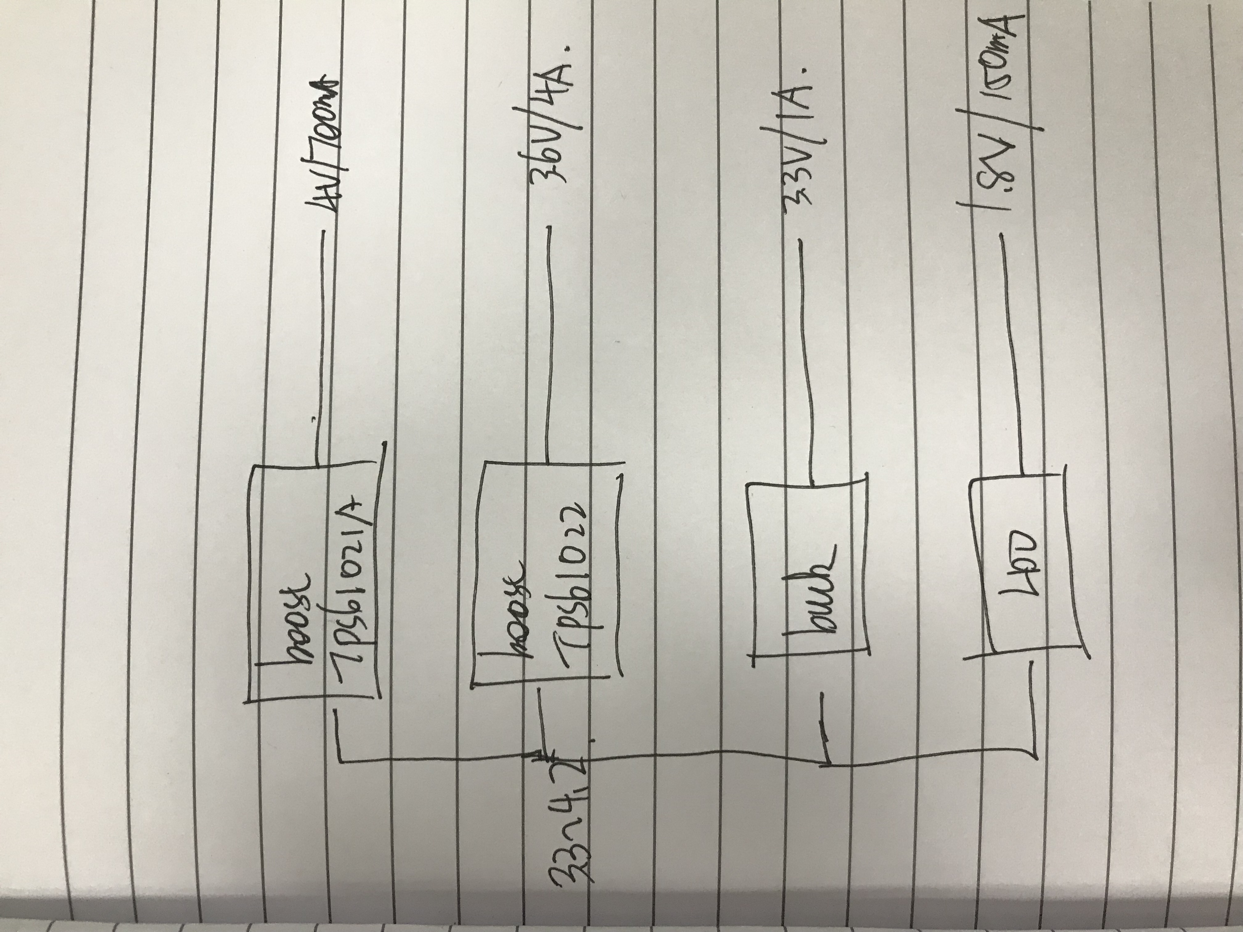
we have a design for below requirement for Boost application.

input voltage: 3.3V to 4.2V
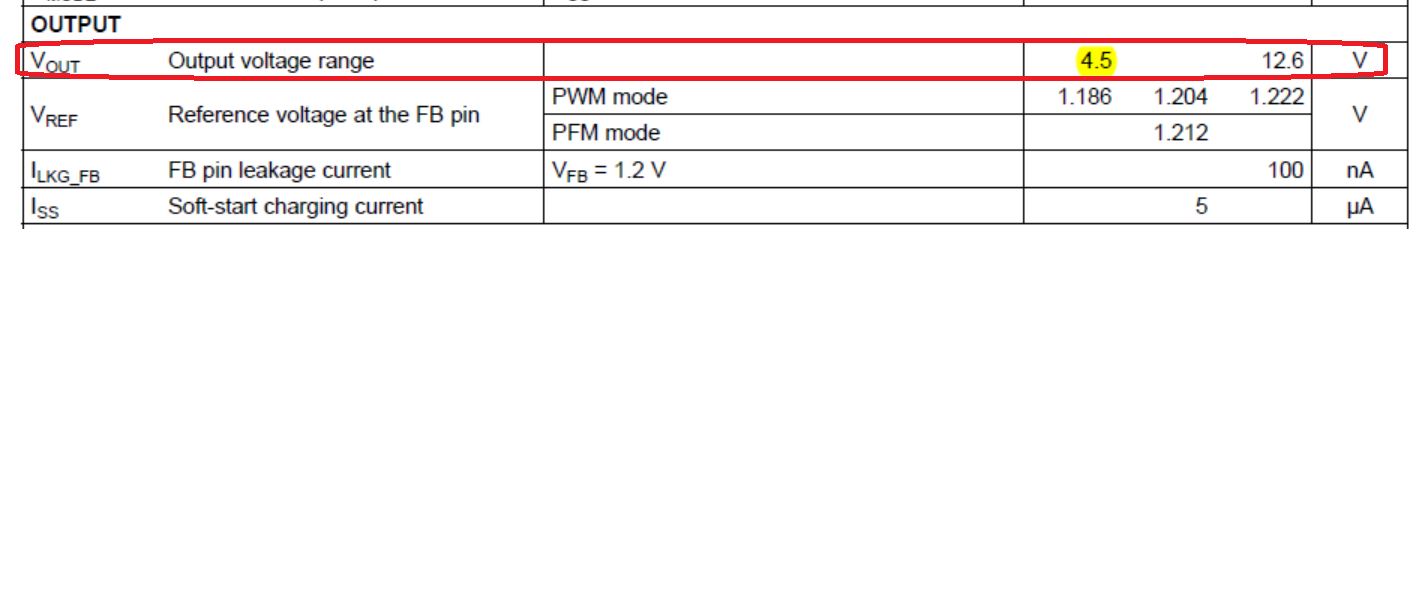
Output voltage: 4V

Output current : 6A

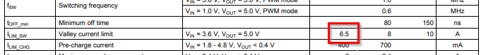
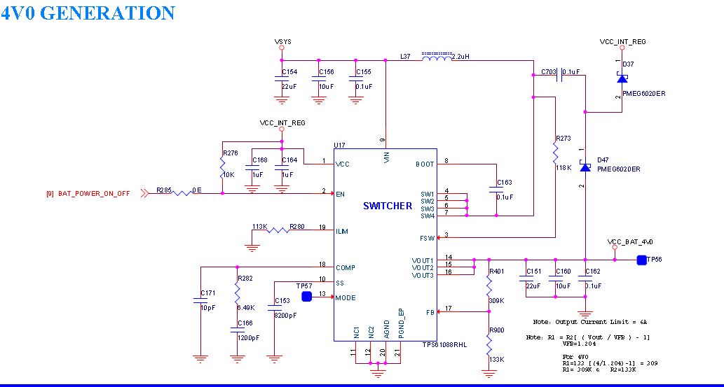
we have chosen TPS61022 ic for our boost design using WEBENCH tools. but these tools only 4A output supported. and TPS61022 Datasheet shown it can be supported up to 8A.

if we go  4V@6A output reqirement then TPS61022 is suitable or not.

please reply as soon as possible.

  • Hi Rajesh,

    Please note that 8A is a typical valley current limit as specified in the datasheet and not the maximum load of the device.

    We have kept the valley current limit to 6.5A which is the worst-case scenario.

    Even if max Iout is increased to 8A, the design fails for the condition shared by you as it violates the valley current limit.

    Regards,

    Atul

  • Hi Atul,

      Valley current limit means inductor current not output current, You could estimate it as input current.

      For your application, you could use TPS61088.

      Could you share your application? Why do you need 6A output?

      Best,

      Jing

  • hello jing,

    thanks for a quick response.

    For your application, you could use TPS61088.

    Rajesh-->> our requirement is output 4V@6A  and this booster minimum output voltage is 4.5V.

    Could you share your application? Why do you need 6A output?

    Rajesh-->> our application is we need 4V@6A output.

                      for that 4V@6A we make below a voltage requirements

    1) 3.6V@4A  using LDO

    2) 4V@700mA  

    3) 3.3V@1A  using Switcher

    4) 1.8V@150mA  using LDO and make from 3.3V input

    please suggest booster for our application is below

    Input Voltage: 3.3V to 4.2V

    output voltage: 4V

    output current: 6A

    we are looking for a low cost solution.

    we are waiting for your soonest reply.

  • Hi Rajesh,

      For your application, I suggest you could use as below power tree. TPS61021A and TPS61022.

      Could you share your application? What is end equipment? I am interested in it.

  • hello jing,

    thanks for a quick reply

    we have already finalized our other part form TI.only one boost converter is pending.

    please suggest 4V@6A output for boost application part & if any alternate available then share.

  • Hi Rajesh,

      For 4V/6A, you could use TPS61088 and add a charge pump to power VCC. and then you could set Vout=4V.

  • hello jing,

    Thanks for a quick response.

    how does this circuit work? can you explain in details?

    if any reference design, you made this type of circuit for better understanding.

    we are waiting for your soonest reply.

  • hello jing,

    Any update?

     please reply ASAP.

  • Hello jing,

    we are waiting for your reply.

    if you can share diode and capacitor value then we can mount this part in our board and test this case.

    our project timeline is very very short and we are waiting for your reply in urgent.

  • Hi Rajesh,

      Sorry about the delay. I am a little busy these days.

      From the TPS61088 block diagram, TPS61088 is powered by VCC pin and in the IC, VCC is connected with Vout by LDO. So min Vout is about 4.5V. 

    We could add another power source to VCC to power it. So use the circuit above, it is a charge pump, so VCC pin voltage is double of VOUT(4V), about 8V. You could download TINA module in Webench and do a simulation.

    For C, you could use 0.1uF, for diode, ~10mA is OK.


  • hello jing,

    thanks for a quick response.

    Below replies from my side:

      From the TPS61088 block diagram, TPS61088 is powered by VCC pin and in the IC, VCC is connected with Vout by LDO. So-min Vout is about 4.5V. 

    Rajesh-->>   what is the role of VCC pin in TPS61088? what is the relation between VCC and Vout?  which term is affected Vout(min) voltage?

    We could add another power source to VCC to power it. So use the circuit above, it is a charge pump, so VCC pin voltage is double of VOUT(4V), about 8V. You could download TINA module in Webench and do a simulation.

    Rajesh-->> I understand charge pump circuit but if we generate 8V at VCC pin then how the output is 4V possible?

                       if we can generate 4V output then we can set divider across FB pin, Right.

    For C, you could use 0.1uF, for diode, ~10mA is OK.

    Rajesh--> thanks for the suggestion for Value of Charge pump circuit.

     we are waiting for your reply  ASAP.

  • Hi Rajesh,

      I find a similar TI design. (TIDA-050021). I think it will be helpful. In the design, charge pump output connects to VIN pin, it will be better than connected to VCC. 

      In the IC, we will choose the max voltage between VIN pin and VOUT pin, and then following a LDO to connect VCC pin, IC uses VCC pin to power the device. IC needs a higher voltage to drive internal MOS, so if we make VCC higher, Vout could be down to 4V.

      Best,

      Jing

  • hello jing,

    As per your suggestions we have added a charge pump circuit to TPS61088 ic. 

    Please review the below schematics.

    Input voltage :  3.3V to 4.2V

    output voltage: 4V @6A

    we are waiting for your reply ASAP.

  • Hi Rajesh,

      From my side, it is better to connect R276 to VSYS not VCC_INT_REG.

    Forward to  AE Helen,

    Hi Helen,

      Do you have any comment?

      Best,

      Jing

  • Dear Sir,

    Why you connect the output of the charge pump to the Vcc pin?  It should be connected to the Vin pin, like what TIDA-050021 done.

  • Hi Jing,

    Please see below App note -

    https://www.ti.com/lit/ug/tiduel6/tiduel6.pdf

    considering the App note, Charge Pump is used to support the Low Input Supply range in case of Super CAP.

    I still do not understand why we need the Charge pump where my Input supply will be stable between 3.1V to 4.2V.

    Because when I am checking the App note, there are Feedback resistors used to generate the 4V output but seems like Charge Pump has nothing to do with the Output Voltage,

    I also have tried in one of my board with just changing the Feedback resistors and I am getting the 4V output.

    Can you please solve this mystery?

    Thanks

    Saumil

  • Hi Saumil,

    Because for the TPS61088, the internal logic & driver circuit is supplied by the Vout when Vo>Vin. And the minimum diver voltage requirement is >4.5V: which means either Vin or Vo should be >4.5V.

    Please check the below block: since Vo is too low, we need to charge pump the Vin pin voltage.

  • Hi Helen,

    Based on the datasheet, the minimum Input Voltage range supported by the TPS61088 is 2.7V.

    It does mean if my minimum input is 3.1V then it can generate 4V without any Charge pump.

    Can you please relook it?

    It seems like there is a lot of confusion created on this but our input voltage never go below 2.7V where we need the Charge pump.

    Thanks

    Saumil

  • Dear Sir,

    Please check the below picture from the datasheet: Vout need to >4.5V, the main reason is to make sure the internal supply voltage is not too low.

  • Hi Helen,

    Everything is confusing.

    I agree with you that min voltage can be generated 4.5V with TPS61088 and that is why we came to TI that how shall we use the same boosted for 4V?

    Can you please check the below link?

    https://www.ti.com/lit/ug/tiduel6/tiduel6.pdf

    Why did this say that to increase the input supply range charge Pump has been used and the Feedback used is for 4V calculation?

    Why feedback resistors not calculated for 4.5V in that case?

    Thanks

    Saumil

  • Hi Saumil,

    It is not conflict.

    1. to get 4V output voltage, we must set the feedback resistor at 4V;

    2. When Vo=4V, the internal supply voltage is not enough(because input voltage also below 4V results low Vcc voltage, Vcc<4V), so we need to find a solution .

    3. To make sure Vcc>4.5V, we need to make  Vin pin voltage >4.5V(because Vo set at 4V, we can't change Vout), for the TPS61088, Vin pin can be seperated with the power input. So we need to found an >4.5V external supply to supply the Vin pin.  Making Vin pin voltage >4.5V, best >5V, then the problem solved.

    4. How to make Vin pin voltage >5V? ...... We found if we add a charge pump circuit, then the Vin pin voltage can be around 2 times the Vout. which is around 8V in this case. So the problem solved!

    noted: charge pump output must connect to the Vin pin, not the Vcc, because the abs max Vcc voltage should be <7V. So it is safe to connect to Vin. 

  • Hi Helen,

    One more thing-

    reliability point of view - how these adjustments are reliable?

    How confident TI on these settings to make the same boosted works for 4V, 6A?

    Because we are planning for Mass Production of 50,000 units we are producing in March 2020 and 500K in 2020-21.

    So, we need to make sure that this given solution works in each and every condition and will not fail anyhow.

    Let me know the reliability so we shall proceed with this given solution and submit the final schematic for review.

    Thanks

    Saumil

  • Dear Saumil,

    Since the charge pump output is added at the Vin pin, and the Vin's maximum stress can be 12V, so it is sure to be OK!

    This is just a small analog circuit. Which is very commonly used in the power supply design. 

    For the TPS61088,  its Vin pin support external supply voltage(Vin pin can be connect to either the power input or the external power supply), many customers, especially for the super cap input application(Vo=3.3V), they supply the Vin pin by an external 5V-6V voltage. Please read the TI design PMP9772

    So the reliability will not be effected. 

    Since your volume is big. I suggested we can have an email review(I'll involve our marketing guys) instead of the E2E review. it is not convenience review through E2E.

    I'll send a message to you.