Other Parts Discussed in Thread: TPS23754, , TPS23753A, TL431
To whom may it concern.
Hi, I'm HS.
I've designed the PoE PD circuit which is using TPS23754 and referenced PMP6812.
I've got some questions about PMP6812.
Since I'm new to this PoE design, Please bear with me and explain and spare you knowledge with me as detailed as possible.
Thank you for your hard work in advance.
1. VC
I've read VC is the bias voltage for DCDC Controller in the chip, TPS23754. But it's from the Tertiary winding.

1-1. I wonder why VC is derived from Tertiary winding?
1-2 What's the purpose of D13, R7 and? C22
I asssume R7 and C22 make LPF for suppressing the voltage spike when the signal in TRANSFORMER which has tertiary winding. Am i correct?
How do you calculate the value of these RCs?
1-3. What's the purpose of R8, R9, R10?
Especially, I'm confused with R9 and R10 because i can't tell which one is for current sensing, I assume R10 is the current sensing resistor tho..
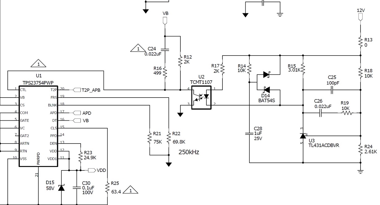
2. Feedback

2-1 I wanna know the role of C24, R16, R12. How do you calculate their proper value??
2-2. I've read VB is 5.1V. Would it be ok if I connect a LED to VB for 'Power On' LED? Or should I connect LED to V_OUT(=12V)?? Which one would be better?
2-3. Basically, I just don't understand how U3 works. This forum and datasheet said it's feedback circuit tho Would you break it down little bit more?
2-4. Does opto-coupler(U2) play a key role in efficiency? I mean, can we maximize the efficiency if we use kinda better opto-coupler than TCMT1107?
Also, Please let me know how you set the RCs for U2
2-5. I read datasheet about BLNK, so called blanking but It was a 'Hm...' You may think I don't know how the game goes and you're dang right lol But yeah here we are,
Would you explain what blanking is and why it is important and how it works??
3.OR-ing

I tried to find information about this DC JACK circuit.
I read some application reports and datasheets including SLVA306A but none of them are same as this design.
Would you enlighten me?? What's going on here?