This thread has been locked.
If you have a related question, please click the "Ask a related question" button in the top right corner. The newly created question will be automatically linked to this question.
Tool/software: WEBENCH® Design Tools
Hi sir,
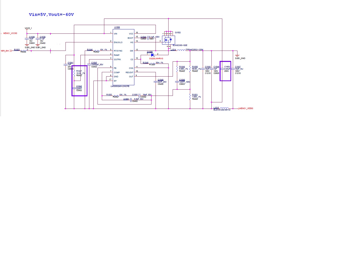
I have created a design using the LM5088 by WEBENCH.
Vin =5V , Vout = -60V, Iout =100mA.
The following are the parameters setting and schematic we followed the suggestion from tool. However, Vout can't get -60V....
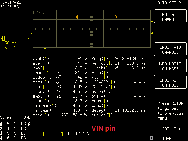
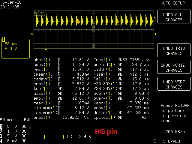
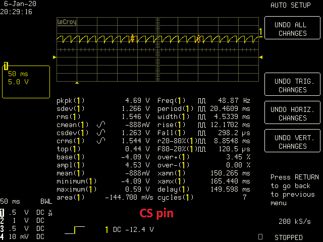
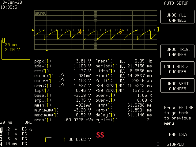
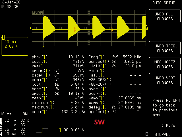
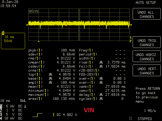
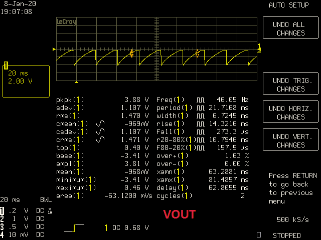
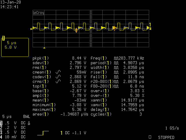
Here are CS/HG/SW/VIN pin status fyr.
It will be appreciated if you can help to check and give me some suggestion. Thanks in advance.
Regards,
Roger
Hi Roger,
How do you apply Enable signal to LM5088?
EN pin to GND voltage must be below 14V, you need to use level shift circuit or zener clamp circuit to limit EN pin to GND pin voltage below 14V, otherwise device maybe damaged once output reach -60V !!
the SW node should swing from 5V to -60V at normal operation.
Pls also current sense resistor to 100mohm for debugging.
B R
Andy
Hi Andy,
The control voltage of EN pin is 3.3V.
We modified current sense resistor from 30m ohm to 100m ohm, the result is the same.
we can not get -60V.
Regards,
Roger
Hi Roger,
the EN control voltage 3.3V is referred to input 5V GND? or referred to output -60V (same as LM5088 GND)?
Hi Andy,
EN control voltage 3.3V is referred to input 5V GND and 5V GND is the same LM5088 GND.
Regards,
Roger
Hi Andy,
I correct my answer about EN pin control issue.
EN pin control voltage 3.3V is referred to input 5V GND.
Regards,
Roger
Hi Roger,
Pls try below:
1. current sense resistor to 100mohm
2. R1553 is NC and R1544=10K & R1545=4.3K mount components
3. Add 100uF 16V Electrolytic cap on 5V input.
4. replace LM5088 with new unused sample.
5. carefully check external component soldering
6. If circuit still not work properly, pls provide waveform of Vin, SS, SW, Vout, and PCB layout.
Hi Roger,
I review your circuit design, Pls make below changes to see if any improvements:
1. R1545=24.9K for Fsw=250KHz,
2. L1514=10uH 3A
3. R1548=33 mohm
4. C1543=0.1uF
5. R1547=10K
6. C1542=150pF
Hi Roger,
The duty cycle is about 93% for 5V to -60V conversion, the Fw should be set below 200KHz, pls make below changes:
1. R1545=30.1K for Fsw=200KHz
2. L1514=15uH >2.5A
3. R1548=33 mohm
4. C1543=0.1uF
Hi Roger,
The duty cycle is about 93% for 5V to -60V conversion, the Fw should be set below 200KHz, pls make below changes:
1. R1545=30.1K for Fsw=200KHz
2. L1514=15uH >2.5A
3. R1548=33 mohm
4. C1543=0.1uF
5. R1553 is NC and R1544=10K & R1545=4.3K mount components
6. Add 100uF 16V Electrolytic cap on 5V input.
Make sure to replace LM5088 with new unused sample.
Let me know if problem can be solved by above.
B R
Andy
Hi Roger,
How about your PCB layout? did you design layout by referring to LM5088 EVM?
I strongly suggest you to apply one LM5088EVM, then modify the circuit and verify your design on EVM.
B R
Andy
Hi Roger,
Pls send PCB layout in seperated layer to me at andy.chen@ti.com.
we can discuss it offline later.
B R
Andy
Hi Roger,
I will close this thread as we are discussing it by email now.
B R
Andy
Hello Andy,
May I ask 1 question? How calculate max. duty in this case? I don't find Max. duty in LM5088 electronic table.
Best Regards,
Kami Huang
Hi Kami,
I just send you Application Note of "Working with inverting buck-boost converters" .
B R
Andy