This thread has been locked.
If you have a related question, please click the "Ask a related question" button in the top right corner. The newly created question will be automatically linked to this question.
Hello.
First of all, I hope you are doing well.
I am trying to do a buck converter that is 48V input and 12V output and 50A output current with a single phase.
I am using 10 mosfets which is 5 of them on the high side and 5 of them on the low side. Low side pins out very well but HO pins out is making a problem.
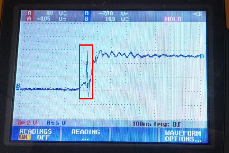
This out shows voltage that is between HighSide mosfet's gate and SW pin.
Why is that happen? I want this part to increase linearly but when it increases one time it goes down and increasing again.
Hi,
This is likely retriggering caused by the MOSFET miller capacitance. Measure SW to GND and LO to GND at the same time as the HO to SW waveform to get a better understanding. Inductance in the gate drive traces may make the problem worse. Also 10 MOSFETs on HO and LO may be too much loading on the pins. In the end you may need some NPN/PNP buffers for the gate drive, and review the VCC current consumption. Start with just one each LO and HO MOSFET, and see if the gate spike occurs. You may need to add a gate resistor to slow down one the transitions.
1. What MOSFETs are you using?
2. What is your switching frequency?
3. Can you share your schematic?
Best Regards,
Bob Sheehan
Power Design Services
Hello Bob,
1- The mosfet's part number is PSMN045-80YS
2- 250kHz switching frequency
3- Is there a way to share this schematic privately?
The waveforms what you want in the below
If I start with 1 HO mosfet and 1 LO mosfet there is a spike waveform seems the other. But when I test with higher output current the spike noise is increasing. It is going worse with output current. The spike with 1HO mosfet and 1LO mosfet in below.
When I use npn pnp drivers for mosfets, the output voltage noise is increasing and the driver's warm is going to high.
Also all these waveforms output was filtered with 20MHz bandwith.
BestRegards
Hello Ali,
at the beginning of this design myself strongly recommended a multiphase solution for 600W buck design,
especially at 48V input voltage at Fsw 250kHz regarding the switching losses. Anyway, some calculations:
- the low side RMS current is 43.38Arms, by 5 FETs 8.7Arms per FET
- the selected FET got 45mOhms RdsON, results in conducted losses 8.7Arms^2 x 45mOhm = 3387mW.
That's way too much for LFPAK package, and I ignored the dead time losses at body diode, those are
high at high currents.
At the high side FETs the situation is even worse, by RMS current 25.05Arms the conducted losses are
less, but you need to consider the switching losses as well, doing this quick & dirty for a single HS FET:
Psw = 1/2 x Vds x Id x tsw x Fsw = 0.5 x 48V x 10A x 10ns x 250kHz = 600mW
Pcond = 5.01Arms^2 x 45mOhm = 1130mW, roughly 1730mW total,again way to much for LFPAK.
(please use Power Stage Designer, Tools, FET losses for detailed analysis)
Seeing the rise and fall times at your low side gate I could see the dead time is good, but tr/tf is not that
promising.
Furthermore the driver power of the ctrl. is distributed to five FETs, so getting gate voltage beyond Miller
plateau is tricky, voltage will drop as soon as FET starts to conduct and Crss reverses to gate.
To avoid cross talking of power loop to gate loops a perfect layout is needed.
We got several Application Notes on this topic online.
To summarize - personally I still think that a multi phase solution is the better starting point.
Going towards four phases at 48Vin / 12Vout duty cycle is 25%, here we have ripple cancellation.
Doing this single phase the RMS stress at input capacitor is 21.71Arms, quite a lot.
Best regards, Bernd
Hi,
I agree with Bernd's analysis and summary. Trying to do this using single phase with your selected FETs isn't going to be the most practical solution.
The switching spike on the high-side gate drive is due to the transition through the miller region with gate drive and layout which is not ideal. Specifically, when the drive voltage reaches the miller plateau, the MOSFET begins to turn on. The switch voltage rises, but due to impedance (inductance) in the driver traces, this pinches off the gate momentarily until the impedance is overcome, at which point the drive voltage begins to rise again.
Using 20 MHz bandwidth for the measurement is masking the problem. You can email me directly with your schematic and a picture of your board. Please include a closeup of your MOSFET and gate drive layout with input capacitor and IC placement.
Regards,
Bob Sheehan
robert.sheehan@ti.com