This thread has been locked.

If you have a related question, please click the "Ask a related question" button in the top right corner. The newly created question will be automatically linked to this question.

PMP10215: PMP10215 schematic issue

Part Number: PMP10215

Hi sir,

I'm in the process of assembling the PMP10215 Rev-D evaluation board, but have encountered a problem.

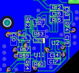
The PCB design has only 56 capacitors, yet the schematic has 57. The schematic shows C100 being located near to Q9,

however the PCB design has C10 near to Q9. Should this capacitor be C100?

The schematic shows C10 being located next to Q5, however it doesn't appear on the PCB.

Also, the PCB layout doesn't have a footprint for C100. Can you please clarify this for me. The PCB manufacturer was very expensive and we don't want to have to make them up again!

Thank you!

  • Hello,

    In the schematic it is described that reference designators ("Ref. Des.") > 99 have been added on the board. That means, C100 is not present on the board and must be added physically. C10 is correctly placed close to Q9, but to a different net.

    So, please, when your board is ready, add C100 capacitor between the collector of Q9 and local ground, physically close to Q9.

    I hope this explain the issue. If not, please let me know.

    Best regards,

    Roberto

  • Hi Roberto,

    Thanks for your reply.

    Sorry, I'm a little confused.

    The schematic says that C100 must be located close to Q9, but the PCB layout has C10 right next to Q9.

    I think what you are saying is that I should place C100 in the location on the PCB where it says "C10".

    However, where then does C10 go? The schematic says that C10 is located next to Q5.

    The PCB doesn't have C10 on it anywhere! There is no footprint available. Thanks

  • Hi Frank,

    I attached below the layout section of Q9-Q10-U2, showing that C10 is close to Q9.

    I hope you have the same revision I have: here on the WEB you should have the schematic in revision D and the board layout in revision B, is that the case?

    Then, according to what I wrote on the schematic, a new 1000 pF ceramic capacitor (named C100, because it doesn't exist on the actual PCB) must be ADDED (this is described on the schematic with the sentence: "Ref. Des. > 99 have been added on the board").

    So, in conclusion, please don't remove C10 and populate it according to the assembly details and BOM, then add an extra capacitor C100, and connect it between the collector of Q9 and local ground (close to Q9).

    Regards,

    Roberto