This thread has been locked.

If you have a related question, please click the "Ask a related question" button in the top right corner. The newly created question will be automatically linked to this question.

Questions about the application for CC2540+RXF2401

Other Parts Discussed in Thread: CC2540

Hello everybody
I am an electrical engineer of KOJ electronic CO. LTD. in China. Recently we developed a 2.4GHz Bluetooth control system by CC2540+RXF2401 chips. The attachments are the relative illustrative electric diagram and the PCB design diagram. And in the electric diagram, the electric line of the inductance L90 and the capacity C’ is disconnected when we let the RXF2401 chip to work. After many tests, we found our control system cannot work normally and our cell phone cannot found the corresponding Bluetooth signal system regularly even though: 1. Using RXF2401 or not; 2. Using the external 2.4GHz antenna or not.
Would you please do us a favor to check our relative diagrams and give us some professional suggestions and advances to solute the questions in our system? I am looking forward to your answer. Thank you very much! Best wishes!
Sincerely yours,
Ken

sheet1.pdfPCB1.pptx

  • AVDD6 (pin 31) is not connected to VDD.

    I have not found a datasheet for RXF2401, is it correct that RXEN should be tied to VDD?

    The layout also has several issues: There should not be traces underneath the RF circuit; The balun should be laid out as in the reference designs; There should not be ground plane or signals underneath the antenna; There should be more ground vias, especially around RF components connected to ground; The ground plane should be solid (not interrupted by signals) between the antenna, balun and the RF chips; I would not recommend using vias on the crystal traces.

    Cheers,
    Fredrik
  • Dear Mr. Fredrik,

    I am Ken from KOJ electronic CO. LTD. in China. First, thank you so much for your helps and suggestions to our project yesterday! By connecting AVDD6 (pin 31) to VDD and using a 2.4GHz external antenna, we found that the CC2540 can work and the system can be connected with our cellphone in some tests. We will follow your advice to develop a new PCB diagram in a few days.  

    Second, I am sorry that I told you a wrong name of the power amplifier chip before. The true name of this chip is RFX2401C. The attachments are the production data sheet of the RFX2401C and the relative 2 files which I mailed before. Since the TXEN of RFX2401C is connected to P12 (pin 7), do I need to make a soft program into the CC2540 in advance to control the high or low level of the signal from this pin?

    I am sorry to disturbing you so much. Would you please continue to check these relative files and give us other professional suggestions about how to use the RFX2401C in our system? I am looking forward to your answer. Thank you very much! Best wishes to you!

    Sincerely yours,

    KenRFX2401C PRODUCTION DATA SHEET.pdf1581.sheet1.pdf3666.PCB1.pptx

  • Hi Ken,


    TXEN is correctly connected to P1_2. All you have to do is to call the HCI_*_ExtendRange* command in SW and the amplifier will be controlled automatically by the stack.

    It will work as it is connected now, but the amplifier will never be turned off. To make the amplifier go into power down when not used you should also connect RXEN to P1_3.


    Best regards,
    Fredrik

  • Dear Mr. Fredrik,

    Thank you for your helps again. TXEN and RXEN have been connected to the relative pins which you suggested in our new electric diagram design.

    My workmate who works on program design has a question about “to call the HCI_*_ExtendRange* command in SW”. He told me that he just placed the function, which is named as “HCI_EXT_ExtendRfRangeCmd”, on the last position of the initialization program part for invoking. And he said he didn’t know what SW means and where it is. Is it OK to do so? Would you please tell us the actually correct position to place these codes? 

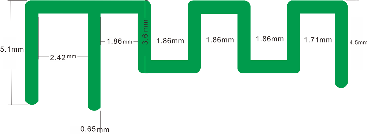
    Second, the attachments are the new relative illustrative electric diagram and the PCB design diagram. Would you please do us a favor to check these files and continue to give us some professional advice? I am still not sure about my new printed antenna design although I have consulted the printed antenna of the TI CC2540 USB Dongle design and other printed antenna designs of some CC2540 application chips. These printed antenna designs are similar but not the same sizes. Would you please tell me the actual referenced sizes of the printed antenna design?

    Third, my program workmate still have an additional question about the CC2540 development. Here it is: “When I try to send data package (only one byte) from Central Device (iPhone, Android and some cell phone) to Peripheral Device (CC2540DK) continually and rapidly(2-3 packages per second), the connection will disconnect automatically. I notice that I can use Without Response mode.

    The key code in Peripheral is as follow:

    static uint8 simpleProfileChar1Props = GATT_PROP_READ | GATT_PROP_WRITE_NO_RSP;

    The key code in iOS is as follow:

    [peripheral writeValue: data forCharacteristic: xxxChar1 type CBCharacteristicWriteWithoutResponse];

    But it seems not work. Would you please tell me how to solve this difficult problem?”

    Thank you very much for your helps these days! I am looking forward to your answer. Best wishes!

    Regards,

    Ken

    Sheet1(new).pdfPCB1(new).pptx ,

  • Hi Ken,

    HCI_EXT_ExtendRfRangeCmd is the right command to use. You can verify that it is working by checking the control signals with an oscilloscope.

    For the data packet question I recommend that you open a new thread so the SW experts can handle it.

    Cheers,
    Fredrik
  • See my comments on the layout in the other thread.

    In the schematic (and the layout) you need to connect pins 2, 3, 4 and 5 of the SMA connector together and to ground. L8 should also be connected to ground.