This thread has been locked.

If you have a related question, please click the "Ask a related question" button in the top right corner. The newly created question will be automatically linked to this question.

Need help for communication between MCU and TRF7960

Other Parts Discussed in Thread: LM3S6950, TRF7960

Dear all,

I'm Huy and I currently work with TRF7960 using LM3S6950.

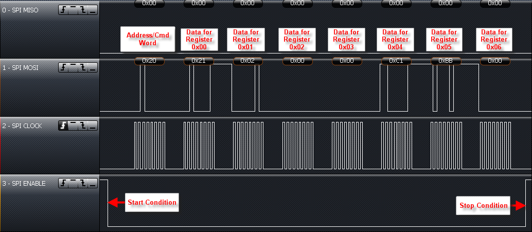
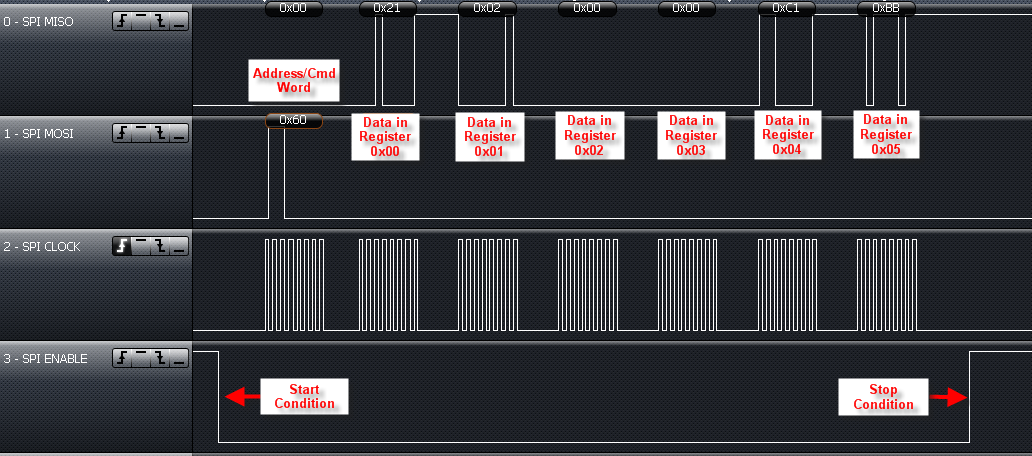
I got a difficult problem that the MCU can not read back any value from TRF7960 (the MISO of TRF7960 is always 0)

I use SPI mode with SS pin for TRF7960

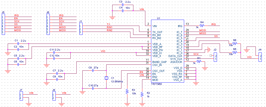
Here is the schematic of my TRF7960 module (I just make it to test the communication with MCU only, so all three pins (pin 5,8,9) of RF are floating)

Here is the code of the MCU to write and read TRF7960's registers:

   SYSCTL_LDOPCTL_R = SYSCTL_LDOPCTL_2_75V ;

   SysCtlClockSet();            // setup PLL

   NVIC_ST_RELOAD_R = (SYS_CLK / SYSTICKHZ) - 1;                     // 1000 SysTick interrupt per second
   NVIC_ST_CTRL_R |= (NVIC_ST_CTRL_CLK_SRC | NVIC_ST_CTRL_ENABLE);   // enable SysTick
   NVIC_ST_CTRL_R |= NVIC_ST_CTRL_INTEN;


   InitializeBoard();                // configure GPIO, SSI, UART, etc

    CLEAR_TRF_EN;     // disable TRF7696 at beginning
    delay_ms(1);
    SET_TRF_EN;
    delay_ms(1);

    command[0] = ModulatorControl;        // select 13.56MHz clock
    command[1] = 0x31;  //13.56 MHz
    WriteSingle(command, 2);

    command[0] = ChipStateControl;       // 3.3V mode
    command[1] = 0x20;
    command[2] = ISOControl;               // ISO15693
    command[3] = 0x02;
    WriteSingle(command,4)

   while(1)                                     // try to read back some registers of TRF7960
     {
         reg[0]=0x00;
         ReadSingle(reg,1);
         reg[0] = 0x01;
         ReadSingle(reg,1);
         reg[0] = 0x02;
         ReadSingle(reg,1);
         reg[0] = 0x03;
         ReadSingle(reg,1);
         reg[0] = 0x04;
         ReadSingle(reg,1);
         reg[0] = 0x05;
         ReadSingle(reg,1);
         reg[0] = 0x06;
         ReadSingle(reg,1);
         reg[0] = 0x07;
         ReadSingle(reg,1);
         reg[0] = 0x08;
        
      }
The MCU outputs SCK, SS, MOSI correctly but MISO is always 0 as shown in the waveform below:

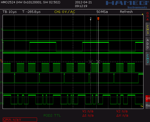
Note: Line15=MOSI, Line14=MISO, Line13=SS, Line12=SCK, Line10=EN

Could anyone help me what is the reason of my problem ?

Thanks,

Huy

  • Huy -

    your schematic looks ok i think - be better to see the antenna, too, later - but i think your biggest issue here is that you are toggling the EN line...just bring it high and leave it there. The SS line is what will select the IC and frame the reads and writes....you know what i mean?

    Also, i have sent you the activation codes twice for the LM3S code, so hopefully you can get that downloaded and have a look so you can get your project going.  

  • Hi Josh,

    Actually, the EN line is always HIGH and is not toggled.

    The EN signal is Line11 not Line10 in the waveform. I made typo mistake in my post. Sorry about that. (Line10 is the waveform of SYS_CLK of TRF7960).

    I think the problem related to digital part of TRF7960 and some possible reasons are:

      1. Power supply for digital part is not available ( due to not good contact to PCB)

      2. IO_0, IO_1 and IO_2 pins are not LOW-HIGH-HIGH for TRF7960 to enter SPI with SS pin mode (due to not good contact to PCB)

      3. Or the 13.56MHz is not working correctly

      4. Finally, TRF7960 is a bad chip (I think it is not the case, just a possible reason!!!)

    For the reason 1, I probed all outputs of internal voltage regulators of TRF7960 (VDD_A, VDD_RF, VDD_PA, VDD_X, VDD_IO) and all of them had correct values specified in the datasheet => It is not the reason 1  (Note, I am sure that VSS_D is connected to GND so that digital part of TRF7960 has good power supply)

    For the reason 2, I measured Ohm of pads between IO_0, IO_1, IO_2  and GND when I firstly assembled TRF7960 to the bare board, there is an amount of resistance => I think they have good contact to PCB. Then I connected IO_0 to GND, and assembled two resistor of 10k to IO_1 and IO_2 to VDD_IO. Finally, I probed voltages at these pins and they are LOW-HIGH-HIGH respectively.

        => It is not the reason 2, I think

    For the reason 3, I probed OSC_OUT pin of TRF7960, there is a 13.56MHz pulses. And I also probed BAND_GAP pin, its voltage is 1.6VDC as you said.

      => I think it is also not the reason 3.

    For the reason 4, I already replaced with a new TRF7960 for a old board that has RF power amplifier stage and made a new module that I showed you in my post. Both of them do not work either (their MISO are always LOW)

      => It is not the reason 4.

    That's all about my thinking and trial to debug it until now @@

    Currently, I have no idea what other reasons are but I am still thinking about it.

    Please help me to how to figure out the reason of my problem.

    PS: I received the activation code to download the reference firmware, I will download it and do my reference to find any problem with my code.

    Thanks

    Huy

  • Huy -

    can you measure your DATA_CLK speed and the SYS_CLK speed? Also, the other thing i am now noticing here is that you are bringing SS line high before you are providing the D_CLKs for the MISO line to respond...

    Should for example look more like this...continuous write

    Continuous Read

    Single Write

    Single Read (this is IRQ Status Register check, but also is an example of Single Read of a Register) 

    thanks!


  • Hi Josh,

    For DATA_CLK and SYS_CLK, they are 1MHz and 30kHz respectively. (I configured SPI's clock to 1MHz)

    I think SYS_CLK should be 60kHz or higher (specified in the datasheet), but my measurement is just about 30kHz !!!

    I did not put SS high before providing DATA_CLK for reading.

    As shown in my waveform, Line13 is the SS signal, and there are 2 set of pulses of DATA_CLK between SS's toggles (I do a "while" loop for many SingleRead)

    => the first 8 pulses of DATA_CLK used to put READ command to TRF7960 and the second 8 pulses of DATA_CLK is used to read back its register value.

     (You can notice that in the second 8 pulses of DATA_CLK, I make MOSI (Line15) all HIGH)


    I have referenced the firmware given by TI, all procedures for SingleWrite and SingleRead are the same as mine but I notice that it configures  weak pull-up resistors for SCK, MOSI, MISO pins.

    => Does MISO need a weak pull-up resistor ?

    Looking forward to your help ^_^/


    Thanks,

    Huy