This thread has been locked.

If you have a related question, please click the "Ask a related question" button in the top right corner. The newly created question will be automatically linked to this question.

the design details about the PCB antenna of the NFC EZ430 Reader Module Reference Design

Other Parts Discussed in Thread: TRF7960, CC2650, CC2640

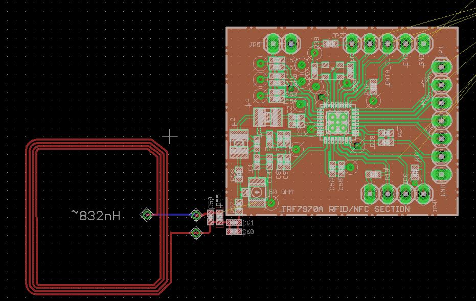
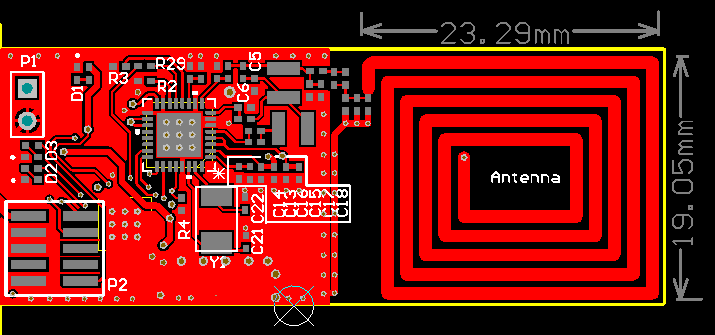
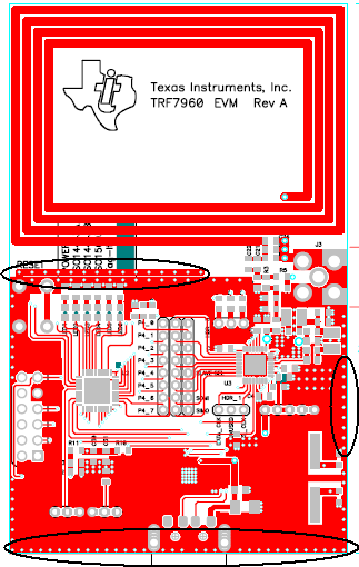
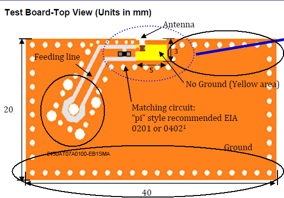
I am a student designing a RFID reader module with the TRF7960. I am trying to make it as small as possible. That means the PCB antenna has to be small enough while still effective.

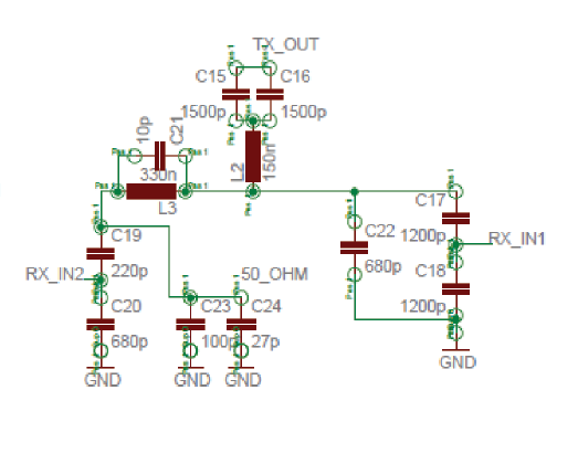
My current design is based on the  TI NFC EZ430 Reader Module Reference Design (www.ti.com/.../TIDM-NFC-EZ430-MODULE). Although the design gerber files is provided, I could not find the corresponding schematic details of the antenna circuit (like information about the shape, trace width, trace spacing, etc.). I am new to PCB antenna design, so I hope to stick to the design reference as exact as possible. Where can I find the information? or is there any design available of PCB antenna at the size of roughly 1.8cm*2.2cm that works with the TRF7960?

My RFID module is supplied at 3.3V.

Thank you very much for any help!


  • the antenna shape was convenient for the form factor - it is just turns on PCB to make inductor which is in range of being able to be tuned to 13.56MHz.

    with that size, if you had 5 turns on each side and used 1mm trace width, with 0x.5mm spacing, you will end up with about 1.3-1.5uH, which will put you in the right area to tune.
  • Hi Josh, thank you for your earlier reply.

    I don't want to create a new post but i have some additional question about the antenna circuitry of the NZ430 Reader Module reference design.

    I was following the reference design schematic of the RF output/receive circuity provided in the TRF7960 datasheet (SLOU186) and also the EVM document(SLOU193), with the output match from 4 ohm to 50 ohm:

    Is there any specification on the trace width of the RF feedline? How does it affect the output impedance? 

    Besides, in my design, the RFID reader module is a subsystem of a greater system with other modules like Bluetooth. What special considerations should be taken into account to ensure there isn't any noise coupling into the supply line?


    BR.

    PHELPS

  • sorry for the delay -

    the lines here are not long enough to worry about the "feedline" impedance. remember that one wavelength at this frequency is ~22m

    you can do something similar like what i did here for a module - i put in heavy ground pour, then on Vin, you just need the recommended caps - for the DC supply itself, you will have to look at see how noisy it is yourself with a scope and make component choices (if needed at all) based on that.   

    you could make this smaller, too - i used 0.100CTR headers on this because i like to have easy connection to logic analyzer, but for production module, these would not be neccesary

  •  

    Josh Wyatt said:

    sorry for the delay -

    the lines here are not long enough to worry about the "feedline" impedance. remember that one wavelength at this frequency is ~22m

    you can do something similar like what i did here for a module - i put in heavy ground pour, then on Vin, you just need the recommended caps - for the DC supply itself, you will have to look at see how noisy it is yourself with a scope and make component choices (if needed at all) based on that.   

    you could make this smaller, too - i used 0.100CTR headers on this because i like to have easy connection to logic analyzer, but for production module, these would not be neccesary

    Thank you, Josh! TI does has the nicest technical support! ^^

    So, based on your first recommendation about the PCB antenna of the TRF7960 in the first reply (5 turns on each side, 1mm trace width and 0.5mm spacing), I came up with something like this:


    Question 1:

    Does the PCB antenna look right to you? because unlike other reference design, this one got little space left on the inside. Would this work?(man, I really have little knowledge on antenna design~....)

    I also have an additional and very related question, if it's not that much trouble. hmm.. I put a CC2640 on the same board as the MCU to control the TRF7960 and to serve as a BLE module. I based the BLE module design on the TI_CC2650 uTag Module design for its compact size and low energy consumption. As a result, I also adopt the RF single-ended configuration and the 2.4Ghz chip antenna (Johanson Technology's  2450AT07A0100)solution. I'm not sure if a chip antenna is somewhat like a PCB antenna, that since the feeding line here is short, I don't need to worry about the trace width of the feeding line. The datasheet of the chip antenna specifies that the feeding line width should be designed to provide 50 Ohm impedance matching characteristics.  

    here's the antenna circuitry schematic and the part of the specification in the antenna chip's datasheet:

    and here is how I did it:

    Question 2:

    I don't really comprehend the notion of "designing the line width to provide a 50 ohm impedance match characteristics" here. Does it refer to the impedance of the feeding line itself that connects the chip antenna, or the total impedance of the matching circuit, or others?

    Question 3:

    I tried to put shielding vias like they did in the TRF7960 EVM design. Is there anyway or universal rule to assess if I put too many of them, or not enough; if I put them in the right place etc.? 


    Really really appreciate your help!!!

    BR.

    Phelps

  • for your HF coil, i would say given the space you have, you should go to maybe 8 turns total and drop width to 0.75mm

    or go to six turns total and drop trace width to 0.5mm


    also, looks like you may have missed the connection to the Slave Select line for the SPI and the caps for VDD_X.

    for 2.45GHz, it totally different story - the parasitic in the layout do affect the overall circuit - best thing to do here is follow exactly what the dimensions are given for the reference circuit and the chip antenna

    when they talk about feedline, they mean the line itself, and it being connected to 50 ohms impedance makes the "match" correctly.

    i am thinking when you say shielding vias, you mean ground vias on the PCB, is that correct? or do you mean for the power pad?
    for the power pad, just follow JEDEC guidance for the RHB package at the end of the data sheet.

    for the PCB itself - i don't think there is a hard and fast rule there - you pay for drill holes - so i think something reasonable would be to make sure you just don't have any islands and make sure you don't have a ground loop.
  • Josh Wyatt said:
    for your HF coil, i would say given the space you have, you should go to maybe 8 turns total and drop width to 0.75mm

    or go to six turns total and drop trace width to 0.5mm


    also, looks like you may have missed the connection to the Slave Select line for the SPI and the caps for VDD_X.

    for 2.45GHz, it totally different story - the parasitic in the layout do affect the overall circuit - best thing to do here is follow exactly what the dimensions are given for the reference circuit and the chip antenna

    when they talk about feedline, they mean the line itself, and it being connected to 50 ohms impedance makes the "match" correctly.

    i am thinking when you say shielding vias, you mean ground vias on the PCB, is that correct? or do you mean for the power pad?
    for the power pad, just follow JEDEC guidance for the RHB package at the end of the data sheet.

    for the PCB itself - i don't think there is a hard and fast rule there - you pay for drill holes - so i think something reasonable would be to make sure you just don't have any islands and make sure you don't have a ground loop.

    I can't believe I skipped the Slave Select line~, thanks for the reminder! As for the VDD_X, it is a output supply. I did not use it to supply the MCU or others (both the TRF7960 and CC2640 are supplied with the same 3.3V VCC ). Do I still have to add the filter caps under this circumstance?

    For the 2.4GHz feed line, I am still sort of confused~~~. So you mean the line itself has to have the impedance of 50 ohm? If so, in order to achieve that, given the related parameters of the PCB board, the trace width will have to be as wide as 2.919mm (as shown in the figure below). That would be unacceptable.  My antenna circuitry schematics is exactly the same as that of the TI_CC2650 uTag design, and the layout is quite similar. And they are both two-layer board. However, the 2.4GHz feed line of the reference design does not appear that wide(of course it might due to the PCB parameter differences).  

     (the antenna part of the reference design)

    As for the shielding vias, I meant the ground vias for the RF feed line (if i understand it right - -...):


    The vias of the two design are rather aligned. Shouldn't they be arranged more separately to avoid forming resonators?

    Many thanks!

    BR.

    Phelps 

  • VDD_X is output regulator and this requires the cap pair as indicated by every reference schematic we have published.
    the ground vias you see in the middle of the TRF EVM are for the UHF antenna that is created on the backside - this was put on the board to demonstrate PCB tracking capability, back when we made EPC Gen2 tag ICs.

    in the CC26xx docuementation, they have layout guidance for both single ended and differential topologies - i would recommend following that to start, then have a detailed look at the reference designs found here, and choose one which is closest to what you are doing.
    www.ti.com/.../technicaldocuments (scroll down to Design Files)
  • I had some success using a small ferrite antenna to read a very small implanted NFC tag. The antenna's not my design - the credit for that has to go to Mathieu at limpkin.fr. If this suits your design it could shrink the size of the reader even more.
    0xfred.wordpress.com/.../
    www.limpkin.fr/index.php

    There's also a commerically available ferrite antenna available
    www.dlpdesign.com/.../fant.shtml

    I did mean to get round to trying a small PCB antenna, but haven't had the time so far.