


Hi,
I am using your CC110L in a design of mine. I am targeting 433MHz. I using reference design SWRR081 as my guide for my design. Schematic is below.
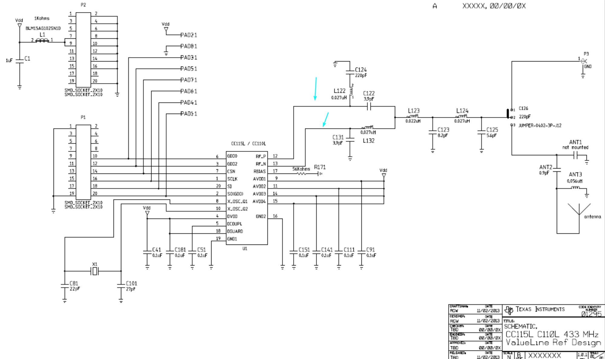
what should the impedance of the RF_P and RF_N traces be (blue arrows pointing to them above)? 50 ohms single ended? I copied the balun component values and placed them exactly as was done in the reference design. My stackup does not line up with what they used though, so I have to be careful about copying their trace widths. The reference design had FR4 with a distance of 31.5mils to the ground plane, mine is also FR4 but a 4-layer stack up so the distance to the ground plane is significantly less (can be anywhere from 5-20 mils as needed for trace widths/impedances).

