I will preface this post by saying that I am a complete beginner when it comes to RF and transmission lines so the problem is probably that there is something I haven't considered.
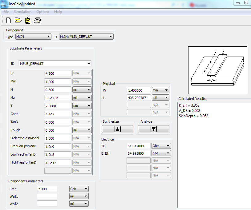
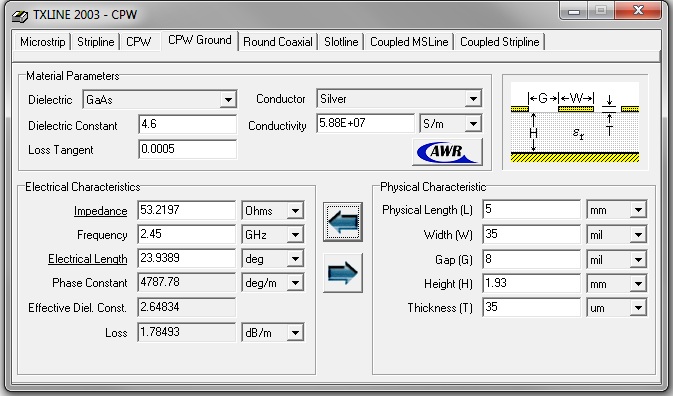
I'm using the CC2500 for a design and I'm a bit confused regarding the 50 Ω line from the matching network to the SMA connector in the 62 mil reference design. I've figured out that this line is a CPWG, Coplanar Wave Guide with Ground, or at least that's what it looks like to me. I used TXLine to calculate the impedance of this line using the 55 mil width and 15 mil spacing from the reference design. I used a dielectric constant of 4.5 for FR4, 62 mil height and 35 µm copper thickness but when inputting this into TXLine (a popular line calculator), I got 55 Ω instead of 50 Ω. If I changed the spacing to 10 mil like I use on the rest of my board, I get as close to 50 Ω as you can get.
Here are some screenshots of TXLine:
http://cl.ly/2P1601093M3h3c200s2c
http://cl.ly/193R3y2h443S2g2L1L37
My question is, should I go by the reference design or by what TXLine says? I assume the reference design is correct but why the descrepancy? I also noticed that the 0.8 mm design seems identical to the 1.6 mm one. The width and spacing of the feed line (is that what you call it?) are identical and the component values of the matching network and balun are identical. Why is this?
Another question while I'm at it... the reference design uses a vertical SMA jack but the one I want to use is an RP-SMA end launch jack. Will this also work as well if I keep the feed line at 50 Ω?