This thread has been locked.

If you have a related question, please click the "Ask a related question" button in the top right corner. The newly created question will be automatically linked to this question.

CC3120BOOST: Clarification on SWPA230 CC3120 Embedded Programming

Part Number: CC3120BOOST
Other Parts Discussed in Thread: CC3120, UNIFLASH

Hello.

Referring to the document SWPA230A – CC3120 and CC3220 SimpleLink™ Wi-Fi Embedded Programming, There are some things I am not clear on.  And would like to get some information, rather that experiment with it and possibly brick it.

First, I have programmed the device using the 31XXEMUBOOST and Uniflash. All works as expected. However we will not be distributing thousands of these programmer boards and the uniflash application to customers nation wide.  So the intent is to program it through the UART on the CC3120, using the above guide.

For initial deveopment, I am simply using a PC based program, and have communicated with the device as expected.

First, to program the device, I assume I use an output from Uniflash?   There are four output files:

  • BIN - Looks like a binary image of something in memory...  This is just a direct image of the FLASH?
  • HEX - ASCII representation, except this file is smaller (??!!)
  • SLI -  Another binary file, for the "image creator"
  • UCF - Another binary file, used by the host

Am I supposed to download the UCF file via the UART through the CC3120 to have it program the FLASH RAM?  Not the SLI?

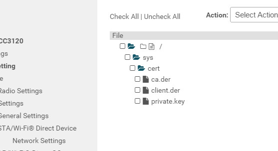
Do these images also contain the files which I added using Uniflash?  For example, the three /sys/cert/...  files ?  Or will those files have to be stored manually (for example, with the API via the SPI bus)?

Next, in document 230, section 5.2 there is a flowchart.  However, in section 5.3 are the individual steps detailed in the flowchart.

Section 5.3.4 states:

To introduce some fixes to the ROM bootloader, it is necessary to download patches to the SRAM. The
procedure for getting information of SRAM storage follows:

(emphasis added)   This states how to get info about the SRAM, but nothing describes anything about the "necessary to download patches..."  What patches?  What is the command to do so?  It just just to section 5.3.5  Raw Storage Erase.   If any "patches" are downloaded to the SRAM, they are erased in this step.

Section 5.3.7 again, says the "ROM is executed together with the programmed patches"  What are the "patches"?

Section 5.3.10 explains that the SFLASH content must reside "in 8 bytes offset of block 33" .  The content cannot fit in 8 bytes.  This means it starts at the 8th byte of block 33, and continues linearly?   There is NOT a need to perform an 8 byte offset at each block, only the first?  

Is the image loaded in step 5.3.6 to load to SRAM the same as the image loaded in step 5.3.10 to load to SFLASH?

Conceptually, is it necessary to load the SRAM ir the SFLASH is also loaded?  Logically, once the SFLASH is loaded, and the device is reset or power cycled, it would boot from the SFLASH, and the SRAM would be purged..?

As I develop more questions, I will follow up.  Thanks.

  • Hi Chris,

    Yes, for embedded programming you will need to use the UCF file output by Uniflash. The UCF file will contain the full contents of the filesystem, including the application binary, certificates, and other other user files you add in Uniflash.

    The patches that are brought up in that section relate to bootloader patches. Similar to how the NWP runs mostly from ROM code but has the ability to load patches through a servicepack, the bootloader can also load patches for its ROM code. When you load download the patches, you are effectively directing the bootloader to use some patches in SRAM. The patches are download in section 5.3.6, using the raw storage write command. Once it has been written, the patch is executed in section 5.3.7.

    Yes, the SFLASH patches should be loaded into flash starting from block 33 with a 8 byte offset, then continued linearly. The SFLASH and SRAM patches are not the same, and both must be loaded. You can think of the SRAM patches being a prerequisite to the SFLASH patches working.

    Let me know if you have more questions on embedded programming for the CC3120. In general, going through the python source files of the TI-provided embedded programming tool is very useful for understanding the programming flow. You can also perform logic analyzer captures of the embedded programming tool as well as Uniflash to see how those tools send the raw bootloader commands to flash the devices. Lastly, I have some debug tips and info in this thread here, in case you run into issues: https://e2e.ti.com/support/wireless-connectivity/wifi/f/968/t/825953

    Regards,
    Michael

  • Michael,

    Thanks but...

    Michael Reymond said:

     The SFLASH and SRAM patches are not the same, and both must be loaded. You can think of the SRAM patches being a prerequisite to the SFLASH patches working.

    Where/What ARE these patches?  I can find no other reference to them except in this document.

    The section 5.x... clearly demonstrates HOW to download the patch (or any binary data for that matter).  But nothing explains Where/What that binary data comes from.

    Updated:  Found them.  I assume they are the PTC files?

    For the SRAM, the doc says to erase 3 blocks, and each block is 4096 bytes (according to the GetStorageInfo) .  

    My GetStorageInfo tells me the SRAM (ID=0) is 4096 bytes X 25 blocks = 100K.  Is this correct?  I haven't found any spec on the M4 CPU in the CC3120 device that says how much SRAM there is. So I have no way of knowing...

    But I am suspect of that as well...  because this same command tells me that the CC3120 BOOST SFLASH (ID=2) has 4096 bytes X 512 blocks = 2Meg.  That is incorrect.  The SFLASH chip on the BOOST board is 16 Meg.  

    Michael Reymond said:

    Yes, for embedded programming you will need to use the UCF file output by Uniflash. The UCF file will contain the full contents of the filesystem, including the application binary, certificates, and other other user files you add in Uniflash.

    I also dug into the binary data of the UCF file. I see four filename entries visible in ASCII... but I find no visible entry for "/sys/cert/client.der"  Although I included that file when I flashed the unit with the EMUBOOST board.  So if it's in that UCF, I can't tell.

    I assume the UCF file is the one used in step 5.3.11?  But at this time I can't even get there since I'm roadblocked on step 5.3.6 and 5.3.10.

    (In the doc, section 5.3.11, the "FS Programming" should be "linked", like the commands are in the earlier sections.)

    I just assume that the "FS Programming" command knows that it's not going to write to wherever those "Patches" are? That it knows where to put the image?  Because the "patches" are loaded into blocks specified in the command.

    So these are the things I am still not clear about.

  • Hi Chris,

    Yes, the patches are the .ptc files you find distributed with the embedded programming tool source.

    When you're using the UART bootloader interface through the embedded programming tool, you're actually communicating with the NWP ARM core. This does have its own separate SRAM from the main 256KB of the M4 ARM core you find on the CC32xx devices.

    The SFLASH size would be correct assuming you're using a 16Mbit flash, which is what is on the CC3120 boosterpack, The command should be returning the size of each block in bytes, not bits.

    Any files you have in uniflash when you create the device image should be added to the generated ucf as well. Note that if you make changes to the files to be programmed in Uniflash, you must click on "Create Image" again to rebuild the device image. Clicking on "Save UCF" only saves the previously-created image.

    The UCF file is indeed the file you use in step 5.3.11

    Yes, using the FS programming API will not overwrite the patches you make in previous steps. This is since while the raw writes will write blindly to the memory address you specify, the FS programming API is a function call to the NWP that is actually very similar to performing a sl_Fs* call with the host driver, as in the NWP will have its own code to handle the file programming request intelligently and extract the needed data from the UCF file and build its filesystem.

    Let me know if you have further questions or need more clarification.

    Regards,

    Michael

  • Michael,

    EDIT: That didn't take long to fail.  See my post following this...

    Michael Reymond said:

    Yes, the patches are the .ptc files you find distributed with the embedded programming tool source.

    When you start with a search on the TI website, you go to the CC3120 chip (that how I started two months ago when I was told to evaluate this chip to integrate it to our product).  Then among the 4 dozen documents, white papers, and notes, there is nothing that directs you to this patch page.  Even the swpa230 doc doesn't tell you what or where these "patches" are.

    Can someone make this less obscure?

    Michael Reymond said:

    When you're using the UART bootloader interface through the embedded programming tool, you're actually communicating with the NWP ARM core. This does have its own separate SRAM from the main 256KB of the M4 ARM core you find on the CC32xx devices.

    Yes, that is obvious by just looking at the boost schematic, and while I am designing the MCU interface to the chip.

    (Why, in doc swas034 document, is NWP an abbreviation for "Wireless Network Processor"?  It is dyslexic ...)

    Michael Reymond said:

    The SFLASH size would be correct assuming you're using a 16Mbit flash, which is what is on the CC3120 boosterpack, The command should be returning the size of each block in bytes, not bits.

    And again, as defined in section 4.4.5 of the doc, if each block size is 4096 bytes, and there are 512 blocks then blocks X bytes = 2meg.  The response I received from the device is (SFLASH):

    00 0a 11   (length and checksum)
    10 00      <-  4096 Bytes    
    02 00      <-  512 Blocks
    00 c2 28 15    (reserved, I know not what this is... )

    Somewhere this is off by a factor of 8.

    Michael Reymond said:

    Any files you have in uniflash when you create the device image should be added to the generated ucf as well. Note that if you make changes to the files to be programmed in Uniflash, you must click on "Create Image" again to rebuild the device image. Clicking on "Save UCF" only saves the previously-created image.

    Yes I did use Uniflash in the correct order.  I created the image, then used the "save" feature.  And saved all four file types.
    1. Add the files...
    2.  Create the image
    3. Save the UCF
    The filenames of my user files are NOT visible anywhere in the UCF.  But other filenames are visible.
    Although I haven't gotten to that stage yet, I am expecting to find they are not in the final burned image...
    As I progress, I will post additional questions as they arise.  So far, cautiously following section 5.3 in small steps is progressing well.  That process is some of the better documentation I've seen.
  • Michael,

    I am attempting to follow steps 1-6 of section 5.3.5.   Here is the communication:

    SECTION 5.3.1
          IN ->00 cc
          OUT->00 03 27 27
          IN ->00 cc
          IN ->84
    SECTION 5.3.2
          OUT->00 03 2f 2f
          IN ->00 cc
          IN ->00 1e 35 01 01 00 03 00 00 00 00 00 00 00 00 00 00 00 00 00 30 00 00 00 00 00 00 00 00 00 00
          OUT->00 cc
    SECTION 5.3.4
          OUT->00 07 31 31 00 00 00 00
          IN ->00 cc
          IN ->00 0a 29 10 00 00 19 00 00 00 00
          OUT->00 cc
    SECTION 5.3.5
    STEP 1  OUT->00 0f 33 30 00 00 00 00 00 00 00 00 00 00 00 03
    STEP 2  IN ->00 cc
    STEP 3  OUT->00 cc
    STEP 4  OUT->00 03 23 23
    STEP 5  IN ->
    

    Per section 5.3.5, step 4,  the host is sending a GetStatus

    In step 5, the device is supposed to respond with an ACK followed by Last Status.

    However, after waiting 15 minutes, nothing is sent.

    Any advice?

  • I was told once that I might get better results if I didn't complain about the poor doc and supports from TI.

    Two weeks later, no help...

    Truth hurts.

    Despite TI ignoring my request for help (three other vendors I've used actually let me open "cases" and communicate directly with engineers,  one even called me, albeit from India, but at least they cared),  I spent my companies time reverse engineering the UART communication with a sniffer, and making it work.

    If anyone comes across this thread  DO NOT PERFORM STEP 3 IN SECTION 5.3.5.  It'll halt the device, and nothing will move forward.

    The remaining steps in this section appear to work correctly.

  • Hi,

    And why you not use Python code as your base for a embedded programming? This code is pretty simple to understand.

    My collogue which was developing for me embedded C# programming code, it take him two days to implement all according documentation provided from TI.

    Jan

  • Hnz said:

    And why you not use Python code as your base for a embedded programming? This code is pretty simple to understand.

    LOL!!  That's pretty funny.  Using Python inside an am335x running TI RTOS.

  • Hi,

    You want to say that rewriting code in Python into C is so hard? I don't agree with this.

    Btw ... I don't see any issue to run Python code at Cortex-A8. Because MicroPython does work pretty well even at Cortex-M3. It is really not a magic.

    Jan

  • We would have to look into compliant JPG and G4 compression, as well as driving a complex FPGA peripheral.  Close to half a million lines of code that is segregated into master projects as well as reusable libraries.

    Not gonna drop everything to do that.