This thread has been locked.

If you have a related question, please click the "Ask a related question" button in the top right corner. The newly created question will be automatically linked to this question.

CC2520: CC2520 ZIGBEE RF Tranceiver IC DVCC and AVCCs decoupling

Part Number: CC2520

Dear TI teams,

I am now designing for a customer to redesign a previous Iot product.

It is using the CC2520  RF TRANSCEIVER  and I am anxious about decoupling.

The customer's design power line was DVDD and AVDD common RFVCC( 3.3V).

RFVCC line is through ferrite beads from D+3.3V line.(TI reference design is shown below)

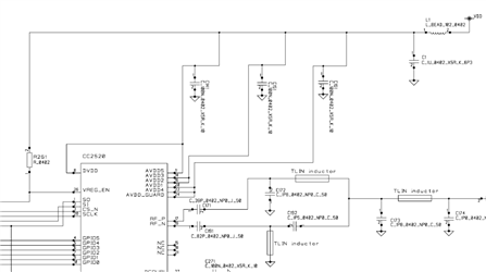
And decoupling condenser is 0.1uF each pair same as TI reference design.

But I think DVDD would be better to separate and connect to +3.3V

and decoupling at +3.3V, because to avoid digital noise to RF signal.

(schematic and power line name is shown below).

Could you please tell me it may be a good idea or bad idea ?

Best regards, Yoshiaki Maehara

  • Dear Yoshiaki, 

    Your layout with the separated +3.3V would work, however we do recommend our layout (with the components sharing a 3.3V) because the ferrite beads reduce noise on that shared line.

    Regards,

    Beste

  • Dear Beste-san

    Thank you very much for your quick reply.

    I am relieved to hear the DVDD  separated +3.3V would also work.

    Then, I would like to change design following your recommendation that DVDD and AVDDs are connected to same line thru ferrite beads.

    But I'm afraid when DVDD line emits clock noise, those noise effects RF signal.

    I'm anxious about it might appear as low band spurious signal or interfere with the receiving signal.

    This is the reason I thought DVDD might be separated with AVDD that is thru ferrite beads.

    Could you please tell me about this issue more detail, if you could ?

    Your assistance is highly appreciated.

    Best regards,

    Yoshiaki Maehara

  • Dear Yoshiaki,

    Following the TI's reference design schematic and PCB layout should be sufficient for preventing interference from noise. For better results, I recommend placing the decoupling capacitors close to the device pins and also giving each capacitor their own via to ground.

    Regards,

    Beste

  • Dear Beste-san

    Thank you very much for your reply.

    I understood that due to your kind explanation.

    You mean it is better to follow TI reference design,  because it is well tested, right?

    And I would like to consider about place condensers closely to the IC pins and populate more decoupling condensers each pins following your advice.


    Thank you very much for your advice again.

    I would like to  close this  thread.

    Best regards,

    Yoshiaki Maehara