This thread has been locked.

If you have a related question, please click the "Ask a related question" button in the top right corner. The newly created question will be automatically linked to this question.

CC2652P: Range only 5m

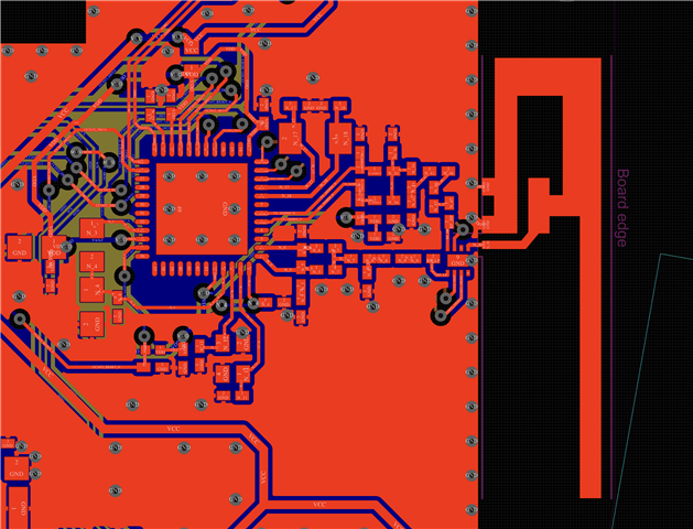
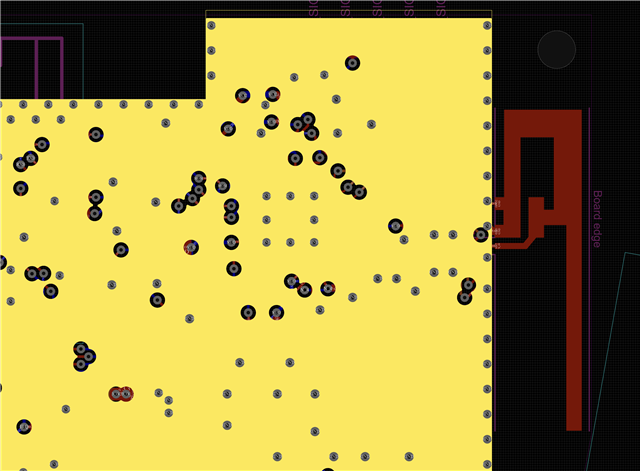
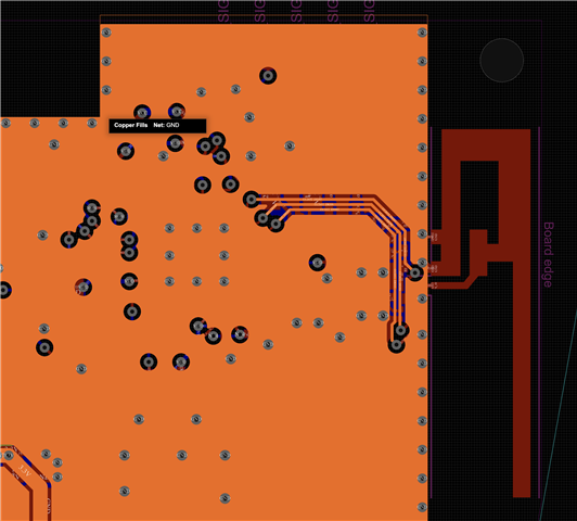
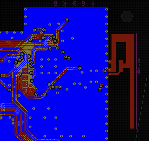
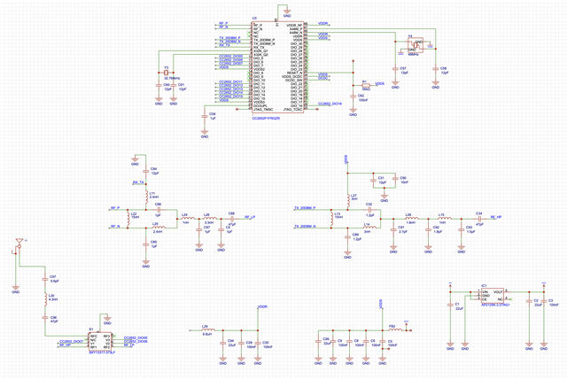
Part Number: CC2652P

Hey guys,

I created a PCB containing a CC2652P in order to develop a Zigbee coordinator working as ZNP. So far everything works good, just the range while transmitting and receiving is really low. I tested multiple Zigbee end devices and the range never got over 5m even in the same room. I already tried different TX power levels, low power (0dbm, 5dbm) and high power (14dbm, 19dbm, 20dbm). The range did not change with different power levels.

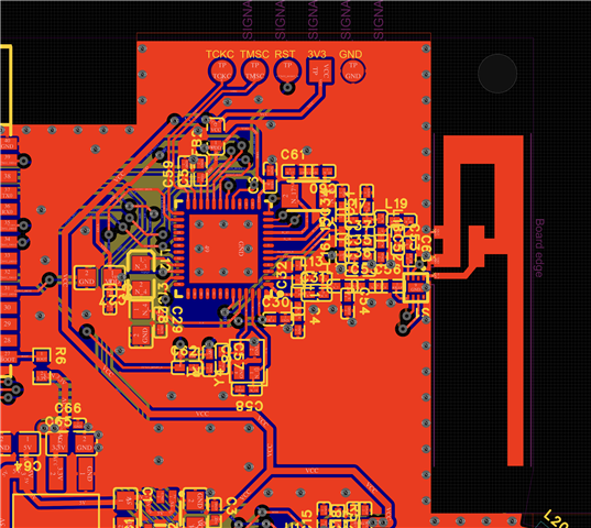
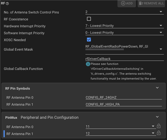
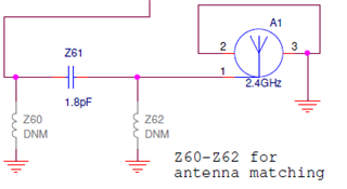
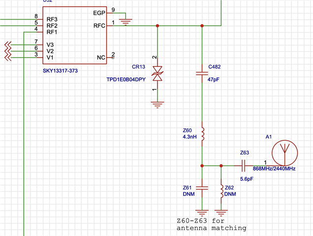
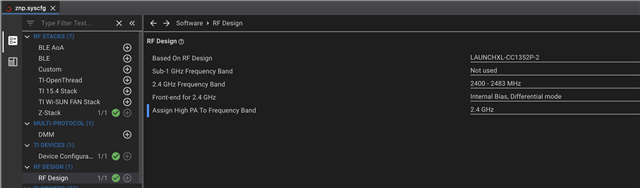
I also already noticed I made a mistake while PCB design, the RX_TX bias pin is not connected as it should be in the reference design. To compensate that I set the RF Frontend in Code Composer Studio to "Internal Bias, Differential Mode".

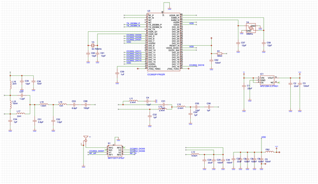
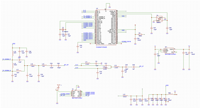
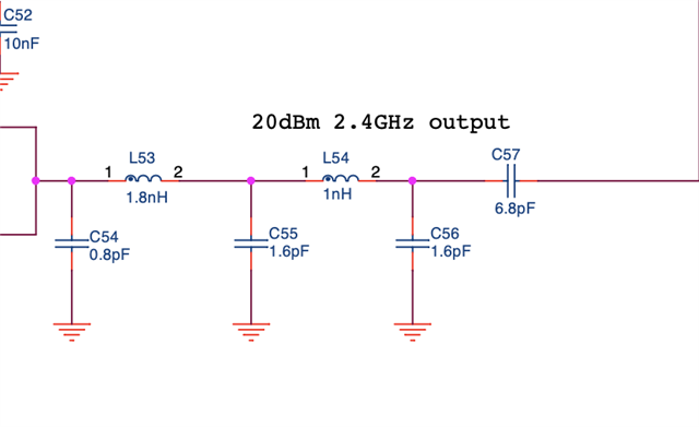
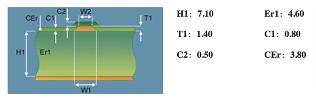
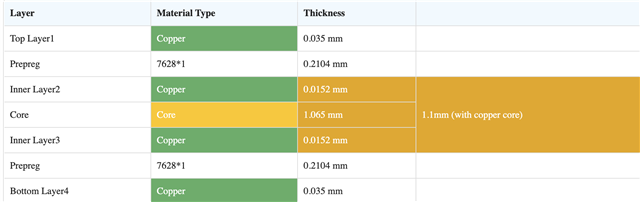
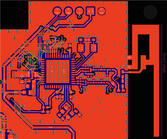
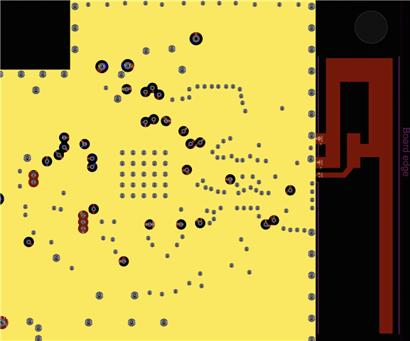
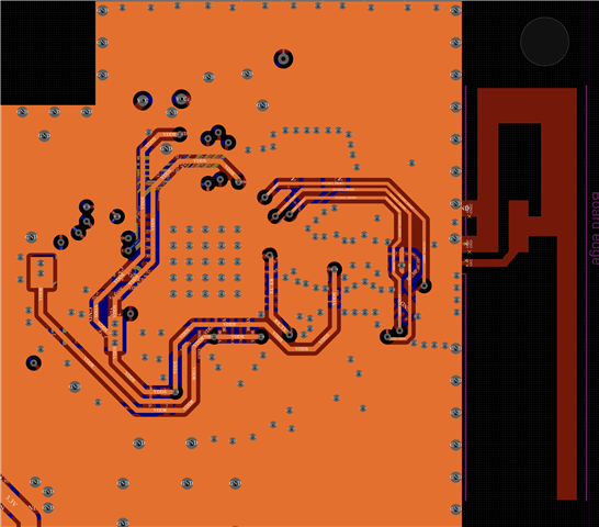
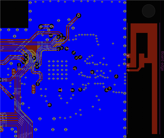
I would be thankful to get some ideas why the range is so low. Schematic and Layout:

  • Hi Sebastian,

    I noticed a couple of items that are different from our reference design and there's some information from the schematic above that's missing.

    1. Have you performed conducted measurements or only radiated? It is best to start with conducted to make sure you're getting the expected output power without the additional complication of the antenna. Sww SWRA640F section 12.3 www.ti.com/.../swra640g.pdf
    2. When you made the changes to the GPIO used for the RF switch was your software project updated accordingly?
    3. You left off the antenna matching network on your schematic. This is important for optimizing the design.
    4. The RF path doesn't look well optimized although it's really difficult to tell from the single screenshot provided. Make sure that the RF path is 50-ohm. The components for the balun and filter should be placed as close as possible to the IC
    5. What does the PCB stackup look like, you only show one layer above, what about the reference plane for the RF path?
    6. What reference design did you base your schematic on?
    7. What voltage are you biasing the 20dBm path with?
    8. Your 5dBm path has a 1pF series capacitor which should probably be a parallel cap to ground, what was the intention there?
    9. Likewise your 20dBm path has a 6.8pF series capacitor.

    I would start by removing the capacitors mentioned in 8 and 9 above and performing your conducted measurements to make sure you're getting your expected output. Then once you know your getting the expected conducted performance go back to your range testing and RF performance.

    Jake

  • Thank you very much for your response.

    1. We did not do conducted measurements yet.

    2. Yes, we updated the firmware according to that.

    Fullscreen
    1
    2
    3
    4
    5
    6
    7
    8
    9
    10
    11
    12
    13
    14
    15
    16
    17
    18
    19
    20
    21
    void rfDriverCallback(RF_Handle client, RF_GlobalEvent events, void* arg)
    {
    /* Switch off all paths first. Needs to be done anyway in every sub-case below. */
    GPIO_write(CONFIG_RF_HIGH_PA, 0);
    GPIO_write(CONFIG_RF_24GHZ, 0);
    if (events & RF_GlobalEventRadioSetup) {
    /* Decode the current PA configuration. */
    RF_TxPowerTable_PAType paType = (RF_TxPowerTable_PAType)RF_getTxPower(client).paType;
    /* 2.4 GHz */
    if (paType == RF_TxPowerTable_HighPA) {
    /* PA enable --> HIGH PA
    * LNA enable --> 2.4 GHz
    */
    GPIO_setMux(CONFIG_RF_24GHZ, IOC_PORT_RFC_GPO0);
    /* Note: RFC_GPO3 is a work-around because the RFC_GPO1 (PA enable signal) is sometimes not
    de-asserted on CC1352 Rev A. */
    GPIO_setMux(CONFIG_RF_HIGH_PA, IOC_PORT_RFC_GPO3);
    } else {
    /* RF core active --> 2.4 GHz */
    XXXXXXXXXXXXXXXXXXXXXXXXXXXXXXXXXXXXXXXXXXXXXXXXXX

    3. I created some more labels to make it more clear. 

    4. I turned of some labels, maybe it gives a better view now. I will rearrange components in the next PCB iteration to be as close as possible to the IC.

    5. Layers below look like that:

    6. It is based on CC1352PEM-XD7793-XD24-PA24.

    7. I added the label, it's VDDS.

    8. Yeah that looks like a mistake.

    9. That one is part of the reference design.

  • OK, I see. Thanks for the updates.

    I think it would be best to start by perrforming conducted measurements to make sure you're getting the expected power output based on the settings you apply. Without this step it's hard to do any debugging.

    In addition, some immediate problems I see in the layout are:

    1. I don't think it's feasible to achieve 50-ohm impedence on the RF path unless you have a very large gap between the top layer and the first inner layer. But it's very difficult to say without being able to measure and just from the screenshots. I would check with your board manufacturer to verify your geometry. I think that would generally cause range issues, but not the issue you're seeing where power settings don't change anything range-wsie.
    2. 100 pF cap is for <1GHz path, would make sense to reduce this value to 47pF as per RF switch datasheet or 6.8pF only as per our reference design.
    3. You should have blocking caps on both side of the switch as per our reference design and the switch datasheet, keep in mind for future revisions.
    4. In general, if you're replicating the reference design and expect similar performance it's important to mirror all details. 
      1. For 20 dBm path you're missing a 1.6pF capacitor in the filter
      2. for 5 dBm the 1 pF is in the wrong place as noted above
      3. Taken together this would likely affect compliance as you may not be filtering harmonics sufficiently. Poor matches can also affect total output power which could cause range issue though.

    -Jake

  • Hi Jake,

    again, thank you for your effort. I reworked the design, it now follows the CC1352-P2 reference design.

    I used a trace width of 0.293mm for the transmission lines because my PCB stackup looks like this:

    My layers from top to bottom look like that:

    The new schematic:

    Any feedback is appreciated.

  • Hi Sebastian,

    For the output match for the PCB antenna it should be something like:

    either a PI or T filter. The important thing is to have the footprints for the components as the values will change depending on what's needed to properly match your antenna. Keep in mind that all three components would come after the 47pF DC block capacitor. Currently you have two components in series after the DC block.

    For the layout on the RF path, I usually treat it as a co-planar waveguide for estimating:

    So 'G' in the diagram above needs to be quite small. But again, this is all estimation, your best bet is to work with your board house as they have simulation tools based on their process and materials so that you can have a more accurate geometry.

    Otherwise, it looks better.

    -Jake

  • Hi Jake,

    I copied that setup from the reference design. 

    How much of the RF performance comes from antenna matching? Is it expected to work decent with those default values?

  • Hi Sebastian,

    You're missing the footprints for Z61 and Z62. You'd want to have those placeholders even if they're not populated in case you need them.

    Your question about RF performance has quite a complicated answer so let me refer you to https://www.ti.com/lit/an/swra161b/swra161b.pdf which is an app-note that gives some high level information on antenna theory.

    You're trying to get all of the power from the device to the antenna. That only happens if you have matched impedance all the way through. Mismatches cause reflections which results in power not going to the antenna. A well-matched antenna will see the most power and a poorly matched antenna will see less power. So basically, all of the RF performance is dependent on a good match.

    In terms of those values, those values are for our design, so if the layout exactly matches then those values are appropriate. Changes in the design or putting the device in a case may detune the antenna and change the values required. This is why it's suggested to have the matching network at least for prototyping, so that you can optimize the design.

    When you ask if it will still work, the answer is probably yes but you can't be sure that you're getting the best performance.

    Again, a good first step is to check your conducted performance because that will give you a hint if there's anything upstream from the antenna that is a problem. If you're getting the expected performance, for example measuring 20 dBm when you have the transmit power set to 20 dBm then you know you're on the right track and can start debugging the radiated performance.