• Join
  • Sign In with my.TI Login
Texas Instruments
  • Products
  • Applications
  • Tools & Software
  • Support & Community
  • Sample & Buy
  • About TI
Sample & Purchase Cart Sample & Purchase Cart
  • Search
  • Advanced
TI E2E™ Community
  • Support Forums
  • Blogs
  • Groups
  • Videos
  • 简体中文
  • More ...
TI Home » TI E2E Community » Support Forums » Amplifiers » Precision Amplifiers » Precision Amplifiers Forum » A Query about servo integrators on the "Ref" pin of the INA333 and some other doubts.
Share
Precision Amplifiers
  • Forum
  • Announcements
  • E2E Wiki
Options
  • Subscribe via RSS
Check out
The Signal blog
  • $core_v2_blog.Current.Name

    Grounding Principles

    Posted 1 day ago
    by Bruce Trump
    In a previous blog on supply bypassing , I cautioned that poor...
  • $core_v2_blog.Current.Name

    Handy Gadgets and Resistor Divider Calculations

    Posted 8 days ago
    by Bruce Trump
    Handy gadgets make our engineering life easier—the little...
  • $core_v2_blog.Current.Name

    Chopper Op Amps—are they really noisy?

    Posted 16 days ago
    by Bruce Trump
    Chopper op amps offer very low offset voltage and dramatically...

A Query about servo integrators on the "Ref" pin of the INA333 and some other doubts.

A Query about servo integrators on the "Ref" pin of the INA333 and some other doubts.

This question is not answered
Yash Chitalia
Posted by Yash Chitalia
on Jul 05 2011 17:34 PM
Prodigy30 points

Hi,

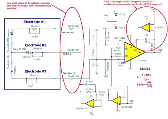
I was looking at a long chain of threads talking about how the reference voltage of the INA333 is set by a voltage divider followed by a buffer and an Integrator circuit.

However, I really haven't understood the importance of the circuit, and whether it is mandatory/recommended to use it. Could someone explain this concept, direct me to a link where this factor has been explained?

Further, what is the recommended input resistance value at each input of the In-Amp for an ECG circuit? (I have attached an image of a circuit used in an older thread, and have highlighted my queries with red circles)


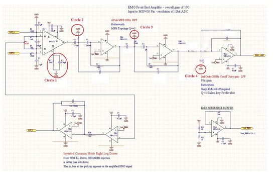
Also, I had certain doubts about a circuit, that was posted later on the same link. I have attached the image of that circuit below for reference.

1. The First stage in this circuit has an IN-AMP which has been referenced to ground, and furthermore, is single supply. So if I understand the circuit correctly, the output of the INAMP will be half wave rectified?

2. Also, now let us assume that the reference pin of the INAMP was given VCC/2 thereby shifting the entire ECG signal by +VCC/2 volts( i.e biasing the ECG signal at half supply). Will the filter stages that follow be referenced to VCC/2 volts in that case? I mean (referring to the figure below) will the GND points in circle 2, circle3 and circle 4 be replaced by VCC/2 points? Or will the Circle 4 GND point remain where it is (since it is the final stage of the circuit, and we want our final signal to be referenced to GND)?


Thanks a lot,

Yash

ECG Amplifier INA333 Integrator
Report Abuse
  • Reply
You have posted to a forum that requires a moderator to approve posts before they are publicly available.
All Replies
  • Matt Hann
    Posted by Matt Hann
    on Jul 06 2011 15:49 PM
    Expert7120 points

    The purpose of the integrator is to act as a high pass filter, driving Vout to the DC value of VREF, thereby removing all of the DC offsets incurred at the front end of the INA (due to VOS, IB*R, CMRR, and especially electrode offsets).

    The resistors that are shown in this circuit are not necessary for proper operation or use of the INA, they are simply there for suggested protection.  According to AAMI EC11: 1991 section 3.2.9 and EC13: 1992 section 3.2.9.2 the filter resistance added to the inputs of the instrumentation gain amplifier must be larger than 100k ohms to keep input currents that could be generated during a device fault or EOS condition to a safe level for the patient.  These requirements are specifically for clinical ECG systems but there may be more relaxed requirements depending on the end application of which I am not aware.

    With regard to the circuit you have referred to in the link--you are correct that if the INA is not referenced to a mid supply DC voltage there could be clipping at the output of the INA for signals that go below ground.  If each of the successive filter stages is DC biased at the non-inverting input at VCC/2, your overall signal will swing about this voltage.  Keep in mind that even if all of the circled grounds that you have shown were referenced to a DC voltage, these will have no effect on the overall DC bias level because the enitre path for the dynamic signal is AC and the DC voltage is therefore seen as an AC ground.  To summarize, in the circuit that you referenced in the link circle 1 (the reference voltage) is really the only one that needs to be reference to VCC/2.

    I hope this helps.

    Matt


    Report Abuse
    • Reply
    You have posted to a forum that requires a moderator to approve posts before they are publicly available.
TI E2E™ Community
  • Support Forums
  • Blogs
  • Videos
  • Groups
  • Site Support & Feedback
  • Settings
TI E2E™ Community Groups
  • TI University Program
  • Make the Switch
  • Microcontroller Projects
  • Motor Drive & Control
Other Communities
  • Deyisupport
  • Designsomething.org
  • beagleboard.org
  • TI on Element 14
  • TI on TechXchangeSM
Other Technical & Support Resources
  • WEBENCH® Design Center
  • Product Information Centers
  • Technical Documents
  • TI Design Network
  • TI Technical Articles
  • TI Training

All content and materials on this site are provided "as is". TI and its respective suppliers and providers of content make no representations about the suitability of these materials for any purpose and disclaim all warranties and conditions with regard to these materials, including but not limited to all implied warranties and conditions of merchantability, fitness for a particular purpose, title and non-infringement of any third party intellectual property right. TI and its respective suppliers and providers of content make no representations about the suitability of these materials for any purpose and disclaim all warranties and conditions with respect to these materials. No license, either express or implied, by estoppel or otherwise, is granted by TI. Use of the information on this site may require a license from a third party, or a license from TI.

Content on this site may contain or be subject to specific guidelines or limitations on use. All postings and use of the content on this site are subject to the Terms of Use of the site; third parties using this content agree to abide by any limitations or guidelines and to comply with the Terms of Use of this site. TI, its suppliers and providers of content reserve the right to make corrections, deletions, modifications, enhancements, improvements and other changes to the content and materials, its products, programs and services at any time or to move or discontinue any content, products, programs, or services without notice.

Follow Us Texas Instruments on Facebook Texas Instruments on Twitter Texas Instruments on LinkedIn Texas Instruments on Google+
TI Worldwide | Contact Us | my.TI Login | Site Map | Corporate Citizenship | mobile m.ti.com (Mobile Version)

TI is a global semiconductor design and manufacturing company. Innovate with 100,000+ analog ICs and
embedded processors, along with software, tools and the industry’s largest sales/support staff.

© Copyright 1995-2013 Texas Instruments Incorporated. All rights reserved.
Trademarks | Privacy Policy | Terms of Use