


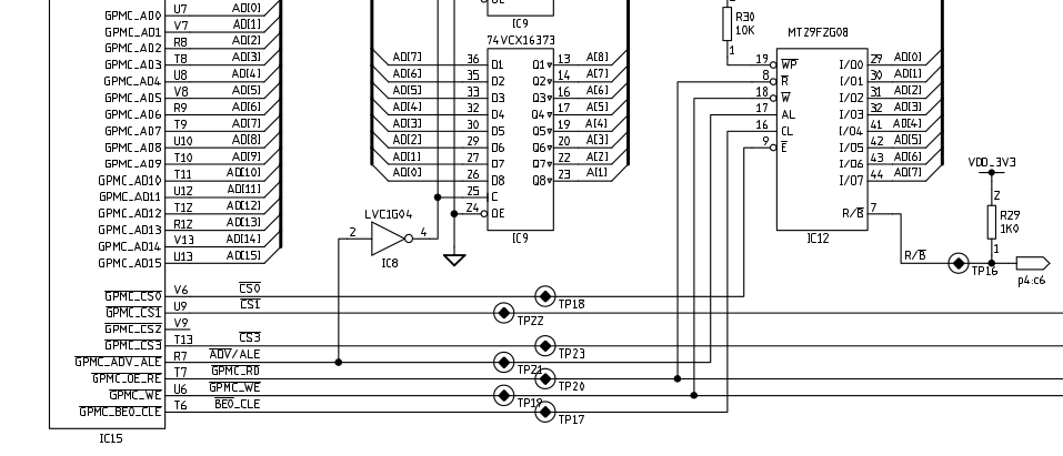
We are developing a custom AM335x board (based on the BeagleBone and AM335x Start Kit) with a Micron MT29F2G08ABAEAWP 2Gbit NAND chip.
This is an 8 bit device, connected to CS0, as follows:-
I have compiled the latest git U-Boot 2013.01, and (with a custom config, board.c and mux.c file - attached below) I am able to boot from MMC (SYSBOOT[4:0] = 10111) :-
U-Boot SPL 2013.01-00291-g9609fad-dirty (Feb 15 2013 - 12:30:45)
OMAP SD/MMC: 0
reading u-boot.img
reading u-boot.img


U-Boot 2013.01-00291-g9609fad-dirty (Feb 15 2013 - 12:30:45)

I2C:   ready
DRAM:  256 MiB
WARNING: Caches not enabled
NAND:  256 MiB
MMC:   OMAP SD/MMC: 0, OMAP SD/MMC: 1
Using default environment

musb-hdrc: ConfigData=0xde (UTMI-8, dyn FIFOs, bulk combine, bulk split, HB-ISO Rx, HB-ISO Tx, SoftConn)
musb-hdrc: MHDRC RTL version 2.0
musb-hdrc: setup fifo_mode 4
musb-hdrc: 28/31 max ep, 16384/16384 memory
USB Host mode controller at 47401000 using PIO, IRQ 0
Net:   cpsw, usb_ether
U-Boot#
I can also write the same MLO and u-boot.img to our NAND device:-
U-Boot#nand info

Device 0: nand0, sector size 128 KiB
  Page size      2048 b
  OOB size         64 b
  Erase size   131072 b
U-Boot# fatload mmc 0 82000000 MLO
reading MLO
75724 bytes read in 14 ms (5.2 MiB/s)
U-Boot# nandecc hw 2
HW BCH8 selected
U-Boot# nand erase 0 200000

NAND erase: device 0 offset 0x0, size 0x200000
Erasing at 0x1e0000 -- 100% complete.
OK
U-Boot# nand write 82000000 0 20000

NAND write: device 0 offset 0x0, size 0x20000
 131072 bytes written: OK
U-Boot# nand dump 0
Page 00000000 dump:
        40 00 00 00 0c 00 00 00  00 00 00 00 00 00 00 00
        00 00 00 00 43 48 53 45  54 54 49 4e 47 53 00 00
        ff ff ff ff ff ff ff ff  ff ff ff ff ff ff ff ff
        ff ff ff ff ff ff ff ff  ff ff ff ff ff ff ff ff
        c1 c0 c0 c0 00 01 00 00  00 00 00 00 00 00 00 00
        00 00 00 00 00 00 00 00  00 00 00 00 00 00 00 00
        00 00 00 00 00 00 00 00  00 00 00 00 00 00 00 00
        ....
But when I switch our board to NAND booting (SYSBOOT[4:0] = 10011), I get nothing on UART0.
Using a scope, I can see that the NAND signals are being toggled (in a burst of activity every 10ms).
The Micron NAND device does have it's own internal ECC hardware, but I think it is OFF by default.
I have tried SYSBOOT[9] at both a '0' and a '1' (to turn ECC mode on / off) but neither mode works.
Can anyone assist me in tracking down what might be wrong ?
Cheers
Mark JACKSON
/*
 * board.c
 *
 * Board functions for Newflow NanoBone board
 *
 * Copyright (C) 2013, Newflow Ltd - http://www.newflow.co.uk/
 *
 * This program is free software; you can redistribute it and/or
 * modify it under the terms of the GNU General Public License as
 * published by the Free Software Foundation; either version 2 of
 * the License, or (at your option) any later version.
 *
 * This program is distributed in the hope that it will be useful,
 * but WITHOUT ANY WARRANTY; without even the implied warranty of
 * MERCHANTABILITY or FITNESS FOR A PARTICULAR /PURPOSE.  See the
 * GNU General Public License for more details.
 */

#include <common.h>
#include <errno.h>
#include <asm/arch/clock.h>
#include <asm/arch/cpu.h>
#include <asm/arch/ddr_defs.h>
#include <asm/arch/gpio.h>
#include <asm/arch/hardware.h>
#include <asm/arch/sys_proto.h>
#include <asm/arch/mem.h>
#include <asm/arch/mmc_host_def.h>
#include <asm/arch/omap.h>
#include <asm/emif.h>
#include <asm/gpio.h>
#include <asm/io.h>
#include <cpsw.h>
#include <i2c.h>
#include <miiphy.h>
#include <spl.h>
#include "board.h"

DECLARE_GLOBAL_DATA_PTR;

/* NAND config */
#define NAND_CS		0
#define NAND_BASE	0x00000000
#define NAND_SIZE	GPMC_SIZE_256M
static u32 gpmc_nand_config[GPMC_MAX_REG] = {
	0x00000800,
	0x001e1e00,
	0x001e1e00,
	0x16051807,
	0x00151e1e,
	0x16000f80,
	0
};

/* FRAM config */
#define FRAM_CS		1
#define FRAM_BASE	0x10000000
#define FRAM_SIZE	GPMC_SIZE_16M
static u32 gpmc_fram_config[GPMC_MAX_REG] = {
	0x00001200,
	0x00101000,
	0x00020201,
	0x0f030f03,
	0x010d1010,
	0x000301c0,
	0
};

/* NOR Flash config */
#define NOR_CS		3
#define NOR_BASE	0x14000000
#define NOR_SIZE	GPMC_SIZE_64M
static u32 gpmc_nor_config[GPMC_MAX_REG] = {
	0x00001200,
	0x00101004,
	0x00020201,
	0x10041004,
	0x010f1010,
	0x000601c0,
	0
};

static struct wd_timer *wdtimer = (struct wd_timer *)WDT_BASE;
#ifdef CONFIG_SPL_BUILD
static struct uart_sys *uart_base = (struct uart_sys *)DEFAULT_UART_BASE;
#endif

/* MII mode defines */
#define PORT1_MII_MODE_ENABLE	0x0
#define PORT2_MII_MODE_ENABLE	0x0
#define PORT1_RMII_MODE_ENABLE	0x1
#define PORT2_RMII_MODE_ENABLE	0x4
#define PORT1_RGMII_MODE_ENABLE	0x12
#define PORT2_RGMII_MODE_ENABLE	0x28

static struct ctrl_dev *cdev = (struct ctrl_dev *)CTRL_DEVICE_BASE;

/* UART Defines */
#ifdef CONFIG_SPL_BUILD
#define UART_RESET		(0x1 << 1)
#define UART_CLK_RUNNING_MASK	0x1
#define UART_SMART_IDLE_EN	(0x1 << 0x3)

static void rtc32k_enable(void)
{
	struct rtc_regs *rtc = (struct rtc_regs *)AM335X_RTC_BASE;

	/*
	 * Unlock the RTC's registers.  For more details please see the
	 * RTC_SS section of the TRM.  In order to unlock we need to
	 * write these specific values (keys) in this order.
	 */
	writel(0x83e70b13, &rtc->kick0r);
	writel(0x95a4f1e0, &rtc->kick1r);

	/* Enable the RTC 32K OSC by setting bits 3 and 6. */
	writel((1 << 3) | (1 << 6), &rtc->osc);
}

static const struct ddr_data ddr3_data = {
	.datardsratio0 = MT41J128MJT125_RD_DQS,
	.datawdsratio0 = MT41J128MJT125_WR_DQS,
	.datafwsratio0 = MT41J128MJT125_PHY_FIFO_WE,
	.datawrsratio0 = MT41J128MJT125_PHY_WR_DATA,
	.datadldiff0 = PHY_DLL_LOCK_DIFF,
};

static const struct cmd_control ddr3_cmd_ctrl_data = {
	.cmd0csratio = MT41J128MJT125_RATIO,
	.cmd0dldiff = MT41J128MJT125_DLL_LOCK_DIFF,
	.cmd0iclkout = MT41J128MJT125_INVERT_CLKOUT,

	.cmd1csratio = MT41J128MJT125_RATIO,
	.cmd1dldiff = MT41J128MJT125_DLL_LOCK_DIFF,
	.cmd1iclkout = MT41J128MJT125_INVERT_CLKOUT,

	.cmd2csratio = MT41J128MJT125_RATIO,
	.cmd2dldiff = MT41J128MJT125_DLL_LOCK_DIFF,
	.cmd2iclkout = MT41J128MJT125_INVERT_CLKOUT,
};

static struct emif_regs ddr3_emif_reg_data = {
	.sdram_config = MT41J128MJT125_EMIF_SDCFG,
	.ref_ctrl = MT41J128MJT125_EMIF_SDREF,
	.sdram_tim1 = MT41J128MJT125_EMIF_TIM1,
	.sdram_tim2 = MT41J128MJT125_EMIF_TIM2,
	.sdram_tim3 = MT41J128MJT125_EMIF_TIM3,
	.zq_config = MT41J128MJT125_ZQ_CFG,
	.emif_ddr_phy_ctlr_1 = MT41J128MJT125_EMIF_READ_LATENCY,
};
#endif

#if defined(CONFIG_NAND_OMAP_GPMC) & !defined(CONFIG_SPL_BUILD)
/******************************************************************************
 * OMAP3 specific command to switch between NAND HW and SW ecc
 *****************************************************************************/
static int do_switch_ecc(cmd_tbl_t * cmdtp, int flag, int argc, char * const argv[])
{
	if (argc < 2)
		goto usage;
	if (strncmp(argv[1], "hw", 2) == 0)
	{
		int type = 1;
		if (argc == 3)
			type = simple_strtoul(argv[2], NULL, 10);
		omap_nand_switch_ecc(type);
	}
	else if (strncmp(argv[1], "sw", 2) == 0)
		omap_nand_switch_ecc(0);
	else
		goto usage;

	return 0;

usage:
	printf ("Usage: nandecc %s\n", cmdtp->usage);
	return 1;
}

U_BOOT_CMD(
	nandecc, 3, 1,	do_switch_ecc,
	"switch OMAP3 NAND ECC calculation algorithm",
	"[hw 1/hw 2/sw] - Switch between NAND ecc algorithm\n"
	"    hw 1 = kernel/FS layout\n"
	"    hw 2 = xloader/uboot layout\n"
	"    sw = 1-bit software"
);

#endif /* CONFIG_NAND_OMAP_GPMC & !CONFIG_SPL_BUILD */

/*
 * early system init of muxing and clocks.
 */
void s_init(void)
{
	/* WDT1 is already running when the bootloader gets control
	 * Disable it to avoid "random" resets
	 */
	writel(0xAAAA, &wdtimer->wdtwspr);
	while (readl(&wdtimer->wdtwwps) != 0x0)
		;
	writel(0x5555, &wdtimer->wdtwspr);
	while (readl(&wdtimer->wdtwwps) != 0x0)
		;

#ifdef CONFIG_SPL_BUILD
	/* Setup the PLLs and the clocks for the peripherals */
	pll_init();

	/* Enable RTC32K clock */
	rtc32k_enable();

	/* UART softreset */
	u32 regVal;
	regVal = readl(&uart_base->uartsyscfg);
	regVal |= UART_RESET;
	writel(regVal, &uart_base->uartsyscfg);
	while ((readl(&uart_base->uartsyssts) &
		UART_CLK_RUNNING_MASK) != UART_CLK_RUNNING_MASK)
		;

	/* Disable smart idle */
	regVal = readl(&uart_base->uartsyscfg);
	regVal |= UART_SMART_IDLE_EN;
	writel(regVal, &uart_base->uartsyscfg);

	gd = &gdata;

	enable_board_pin_mux();

	//gpio_request(GPIO_DDR_VTT_EN, "ddr_vtt_en");
	//gpio_direction_output(GPIO_DDR_VTT_EN, 1);

	preloader_console_init();

	i2c_init(CONFIG_SYS_I2C_SPEED, CONFIG_SYS_I2C_SLAVE);

	config_ddr(303, MT41J128MJT125_IOCTRL_VALUE, &ddr3_data,
		   &ddr3_cmd_ctrl_data, &ddr3_emif_reg_data);
#endif
}

/*
 * Basic board specific setup.  Pinmux has been handled already.
 */
int board_init(void)
{
	i2c_init(CONFIG_SYS_I2C_SPEED, CONFIG_SYS_I2C_SLAVE);

	gd->bd->bi_boot_params = PHYS_DRAM_1 + 0x100;

	gpmc_init();

	/* enable NAND flash chip select */
	enable_gpmc_cs_config(gpmc_nand_config, &gpmc_cfg->cs[NAND_CS],
		NAND_BASE, NAND_SIZE);
	/* enable FRAM chip select */
	enable_gpmc_cs_config(gpmc_fram_config, &gpmc_cfg->cs[FRAM_CS],
		FRAM_BASE, FRAM_SIZE);
	/* enable NOR flash chip select */
	enable_gpmc_cs_config(gpmc_nor_config, &gpmc_cfg->cs[NOR_CS],
		NOR_BASE, NOR_SIZE);

	return 0;
}

#ifdef CONFIG_BOARD_LATE_INIT
int board_late_init(void)
{
#ifdef CONFIG_ENV_VARS_UBOOT_RUNTIME_CONFIG
	setenv("board_name", "NANOBONE");
	setenv("board_rev", "0001");
#endif

	return 0;
}
#endif

#ifdef CONFIG_DRIVER_TI_CPSW
static void cpsw_control(int enabled)
{
	/* VTP can be added here */

	return;
}

static struct cpsw_slave_data cpsw_slaves[] = {
	{
		.slave_reg_ofs	= 0x208,
		.sliver_reg_ofs	= 0xd80,
		.phy_id		= 0,
	},
	{
		.slave_reg_ofs	= 0x308,
		.sliver_reg_ofs	= 0xdc0,
		.phy_id		= 1,
	},
};

static struct cpsw_platform_data cpsw_data = {
	.mdio_base		= AM335X_CPSW_MDIO_BASE,
	.cpsw_base		= AM335X_CPSW_BASE,
	.mdio_div		= 0xff,
	.channels		= 8,
	.cpdma_reg_ofs		= 0x800,
	.slaves			= 1,
	.slave_data		= cpsw_slaves,
	.ale_reg_ofs		= 0xd00,
	.ale_entries		= 1024,
	.host_port_reg_ofs	= 0x108,
	.hw_stats_reg_ofs	= 0x900,
	.mac_control		= (1 << 5),
	.control		= cpsw_control,
	.host_port_num		= 0,
	.version		= CPSW_CTRL_VERSION_2,
};
#endif

#if defined(CONFIG_DRIVER_TI_CPSW) || \
	(defined(CONFIG_USB_ETHER) && defined(CONFIG_MUSB_GADGET))
int board_eth_init(bd_t *bis)
{
	int rv, n = 0;
#ifdef CONFIG_DRIVER_TI_CPSW
	uint8_t mac_addr[6];
	uint32_t mac_hi, mac_lo;

	if (!eth_getenv_enetaddr("ethaddr", mac_addr)) {
		debug("<ethaddr> not set. Reading from E-fuse\n");
		/* try reading mac address from efuse */
		mac_lo = readl(&cdev->macid0l);
		mac_hi = readl(&cdev->macid0h);
		mac_addr[0] = mac_hi & 0xFF;
		mac_addr[1] = (mac_hi & 0xFF00) >> 8;
		mac_addr[2] = (mac_hi & 0xFF0000) >> 16;
		mac_addr[3] = (mac_hi & 0xFF000000) >> 24;
		mac_addr[4] = mac_lo & 0xFF;
		mac_addr[5] = (mac_lo & 0xFF00) >> 8;

		if (is_valid_ether_addr(mac_addr))
			eth_setenv_enetaddr("ethaddr", mac_addr);
		else
			goto try_usbether;
	}

	writel(PORT1_MII_MODE_ENABLE | PORT2_RMII_MODE_ENABLE, &cdev->miisel);
	cpsw_slaves[0].phy_if = PHY_INTERFACE_MODE_MII;
	cpsw_slaves[1].phy_if = PHY_INTERFACE_MODE_RMII;

	rv = cpsw_register(&cpsw_data);
	if (rv < 0)
		printf("Error %d registering CPSW switch\n", rv);
	else
		n += rv;
#endif
try_usbether:
#if defined(CONFIG_USB_ETHER) && !defined(CONFIG_SPL_BUILD)
	rv = usb_eth_initialize(bis);
	if (rv < 0)
		printf("Error %d registering USB_ETHER\n", rv);
	else
		n += rv;
#endif
	return n;
}
#endif
/*
 * mux.c
 *
 * Copyright (C) 2013, Newflow Ltd - http://www.newflow.co.uk/
 *
 * This program is free software; you can redistribute it and/or
 * modify it under the terms of the GNU General Public License as
 * published by the Free Software Foundation version 2.
 *
 * This program is distributed "as is" WITHOUT ANY WARRANTY of any
 * kind, whether express or implied; without even the implied warranty
 * of MERCHANTABILITY or FITNESS FOR A PARTICULAR PURPOSE. See the
 * GNU General Public License for more details.
 */

#include <common.h>
#include <asm/arch/sys_proto.h>
#include <asm/arch/hardware.h>
#include <asm/arch/mux.h>
#include <asm/io.h>
#include <i2c.h>
#include "board.h"

static struct module_pin_mux gpmc_pin_mux[] = {
	{OFFSET(gpmc_ad0), (MODE(0) | PULLUP_EN | RXACTIVE)},	/* GPMC AD0 */
	{OFFSET(gpmc_ad1), (MODE(0) | PULLUP_EN | RXACTIVE)},	/* GPMC AD1 */
	{OFFSET(gpmc_ad2), (MODE(0) | PULLUP_EN | RXACTIVE)},	/* GPMC AD2 */
	{OFFSET(gpmc_ad3), (MODE(0) | PULLUP_EN | RXACTIVE)},	/* GPMC AD3 */
	{OFFSET(gpmc_ad4), (MODE(0) | PULLUP_EN | RXACTIVE)},	/* GPMC AD4 */
	{OFFSET(gpmc_ad5), (MODE(0) | PULLUP_EN | RXACTIVE)},	/* GPMC AD5 */
	{OFFSET(gpmc_ad6), (MODE(0) | PULLUP_EN | RXACTIVE)},	/* GPMC AD6 */
	{OFFSET(gpmc_ad7), (MODE(0) | PULLUP_EN | RXACTIVE)},	/* GPMC AD7 */
	{OFFSET(gpmc_ad8), (MODE(0) | PULLUP_EN | RXACTIVE)},	/* GPMC AD8 */
	{OFFSET(gpmc_ad9), (MODE(0) | PULLUP_EN | RXACTIVE)},	/* GPMC AD9 */
	{OFFSET(gpmc_ad10), (MODE(0) | PULLUP_EN | RXACTIVE)},	/* GPMC AD10 */
	{OFFSET(gpmc_ad11), (MODE(0) | PULLUP_EN | RXACTIVE)},	/* GPMC AD11 */
	{OFFSET(gpmc_ad12), (MODE(0) | PULLUP_EN | RXACTIVE)},	/* GPMC AD12 */
	{OFFSET(gpmc_ad13), (MODE(0) | PULLUP_EN | RXACTIVE)},	/* GPMC AD13 */
	{OFFSET(gpmc_ad14), (MODE(0) | PULLUP_EN | RXACTIVE)},	/* GPMC AD14 */
	{OFFSET(gpmc_ad15), (MODE(0) | PULLUP_EN | RXACTIVE)},	/* GPMC AD15 */
	{OFFSET(gpmc_csn0), (MODE(0) | PULLUDEN)},	/* GPMC_CSN0 */
	{OFFSET(gpmc_csn1), (MODE(0) | PULLUDEN)},	/* GPMC_CSN1 */
	{OFFSET(gpmc_csn2), (MODE(0) | PULLUDEN)},	/* GPMC_CSN2 */
	{OFFSET(gpmc_csn3), (MODE(0) | PULLUDEN)},	/* GPMC_CSN3 */
	{OFFSET(gpmc_advn_ale), (MODE(0) | PULLUDEN)},	/* GPMC_ADV_ALE */
	{OFFSET(gpmc_oen_ren), (MODE(0) | PULLUDEN)},	/* GPMC_OE */
	{OFFSET(gpmc_wen), (MODE(0) | PULLUDEN)},	/* GPMC_WEN */
	{OFFSET(gpmc_be0n_cle), (MODE(0) | PULLUDEN)},	/* GPMC_BE_CLE */
	{OFFSET(lcd_data1), (MODE(1) | PULLUDDIS)},	/* GPMC AD17 */
	{OFFSET(lcd_data2), (MODE(1) | PULLUDDIS)},	/* GPMC AD18 */
	{OFFSET(lcd_data3), (MODE(1) | PULLUDDIS)},	/* GPMC AD19 */
	{OFFSET(lcd_data4), (MODE(1) | PULLUDDIS)},	/* GPMC AD20 */
	{OFFSET(lcd_data5), (MODE(1) | PULLUDDIS)},	/* GPMC AD21 */
	{OFFSET(lcd_data6), (MODE(1) | PULLUDDIS)},	/* GPMC AD22 */
	{OFFSET(lcd_data7), (MODE(1) | PULLUDDIS)},	/* GPMC AD23 */
	{OFFSET(lcd_data8), (MODE(1) | PULLUDDIS)},	/* GPMC AD24 */
	{OFFSET(lcd_data9), (MODE(1) | PULLUDDIS)},	/* GPMC AD25 */
	{OFFSET(lcd_data10), (MODE(1) | PULLUDDIS)},	/* GPMC AD26 */
	{-1},
};

static struct module_pin_mux i2c0_pin_mux[] = {
	{OFFSET(i2c0_sda), (MODE(0) | RXACTIVE |
			PULLUDEN | SLEWCTRL)}, /* I2C_DATA */
	{OFFSET(i2c0_scl), (MODE(0) | RXACTIVE |
			PULLUDEN | SLEWCTRL)}, /* I2C_SCLK */
	{-1},
};

static struct module_pin_mux mii1_pin_mux[] = {
	{OFFSET(mii1_col), MODE(0) | RXACTIVE},		/* MII1_COL */
	{OFFSET(mii1_crs), MODE(0) | RXACTIVE},		/* MII1_CRS */
	{OFFSET(mii1_rxerr), MODE(0) | RXACTIVE},	/* MII1_RXERR */
	{OFFSET(mii1_txen), MODE(0)},			/* MII1_TXEN */
	{OFFSET(mii1_rxdv), MODE(0) | RXACTIVE},	/* MII1_RXDV */
	{OFFSET(mii1_txd3), MODE(0)},			/* MII1_TXD3 */
	{OFFSET(mii1_txd2), MODE(0)},			/* MII1_TXD2 */
	{OFFSET(mii1_txd1), MODE(0)},			/* MII1_TXD1 */
	{OFFSET(mii1_txd0), MODE(0)},			/* MII1_TXD0 */
	{OFFSET(mii1_txclk), MODE(0) | RXACTIVE},	/* MII1_TXCLK */
	{OFFSET(mii1_rxclk), MODE(0) | RXACTIVE},	/* MII1_RXCLK */
	{OFFSET(mii1_rxd3), MODE(0) | RXACTIVE},	/* MII1_RXD3 */
	{OFFSET(mii1_rxd2), MODE(0) | RXACTIVE},	/* MII1_RXD2 */
	{OFFSET(mii1_rxd1), MODE(0) | RXACTIVE},	/* MII1_RXD1 */
	{OFFSET(mii1_rxd0), MODE(0) | RXACTIVE},	/* MII1_RXD0 */
	{OFFSET(mdio_data), MODE(0) | RXACTIVE | PULLUP_EN}, /* MDIO_DATA */
	{OFFSET(mdio_clk), MODE(0) | PULLUP_EN},	/* MDIO_CLK */
	{-1},
};

static struct module_pin_mux mii2_pin_mux[] = {
	{OFFSET(gpmc_a0), MODE(1)},			/* MII2_TXEN */
	{OFFSET(gpmc_a1), MODE(1) | RXACTIVE},		/* MII2_RXDV */
	{OFFSET(gpmc_a2), MODE(1)},			/* MII2_TXD3 */
	{OFFSET(gpmc_a3), MODE(1)},			/* MII2_TXD2 */
	{OFFSET(gpmc_a4), MODE(1)},			/* MII2_TXD1 */
	{OFFSET(gpmc_a5), MODE(1)},			/* MII2_TXD0 */
	{OFFSET(gpmc_a6), MODE(1) | RXACTIVE},		/* MII2_TXCLK */
	{OFFSET(gpmc_a7), MODE(1) | RXACTIVE},		/* MII2_RXCLK */
	{OFFSET(gpmc_a8), MODE(1) | RXACTIVE},		/* MII2_RXD3 */
	{OFFSET(gpmc_a9), MODE(1) | RXACTIVE},		/* MII2_RXD2 */
	{OFFSET(gpmc_a10), MODE(1) | RXACTIVE},		/* MII2_RXD1 */
	{OFFSET(gpmc_a11), MODE(1) | RXACTIVE},		/* MII2_RXD0 */
	{OFFSET(gpmc_wait0), MODE(1) | RXACTIVE},	/* MII2_CRS */
	{OFFSET(gpmc_wpn), MODE(1) | RXACTIVE},		/* MII2_RXERR */
	{OFFSET(gpmc_be1n), MODE(1) | RXACTIVE},	/* MII2_COL */
	{OFFSET(mdio_data), MODE(0) | RXACTIVE | PULLUP_EN}, /* MDIO_DATA */
	{OFFSET(mdio_clk), MODE(0) | PULLUP_EN},	/* MDIO_CLK */
	// CRS/BSY_SEL
	//{OFFSET(spi0_cs0), (MODE(7) | PULLUDEN)},	/* GPIO0_5 */
	{-1},
};

static struct module_pin_mux mmc0_no_cd_pin_mux[] = {
	{OFFSET(mmc0_dat3), (MODE(0) | RXACTIVE | PULLUP_EN)},	/* MMC0_DAT3 */
	{OFFSET(mmc0_dat2), (MODE(0) | RXACTIVE | PULLUP_EN)},	/* MMC0_DAT2 */
	{OFFSET(mmc0_dat1), (MODE(0) | RXACTIVE | PULLUP_EN)},	/* MMC0_DAT1 */
	{OFFSET(mmc0_dat0), (MODE(0) | RXACTIVE | PULLUP_EN)},	/* MMC0_DAT0 */
	{OFFSET(mmc0_clk), (MODE(0) | RXACTIVE | PULLUP_EN)},	/* MMC0_CLK */
	{OFFSET(mmc0_cmd), (MODE(0) | RXACTIVE | PULLUP_EN)},	/* MMC0_CMD */
	{OFFSET(mcasp0_aclkr), (MODE(4) | RXACTIVE)},		/* MMC0_WP */
	{OFFSET(emu1), (MODE(7) | RXACTIVE)},			/* MMC0_CD */
	//{OFFSET(mcasp0_fsr), (MODE(7))},			/* MMC0_PWR */
	{-1},
};

static struct module_pin_mux rmii1_pin_mux[] = {
	{OFFSET(mii1_crs), MODE(1) | RXACTIVE},		/* RMII1_CRS_DV */
	{OFFSET(mii1_rxerr), MODE(1) | RXACTIVE},	/* RMII1_RXER */
	{OFFSET(mii1_txen), MODE(1)},			/* RMII1_TXEN */
	{OFFSET(mii1_txd1), MODE(1)},			/* RMII1_TXD1 */
	{OFFSET(mii1_txd0), MODE(1)},			/* RMII1_TXD0 */
	{OFFSET(mii1_rxd1), MODE(1) | RXACTIVE},	/* RMII1_RXD1 */
	{OFFSET(mii1_rxd0), MODE(1) | RXACTIVE},	/* RMII1_RXD0 */
	{OFFSET(mdio_data), MODE(0) | RXACTIVE | PULLUP_EN},/* MDIO_DATA */
	{OFFSET(mdio_clk), MODE(0) | PULLUP_EN},	/* MDIO_CLK */
	{-1},
};

static struct module_pin_mux rmii2_pin_mux[] = {
	{OFFSET(gpmc_wait0), MODE(3) | RXACTIVE},	/* RMII2_CRS_DV */
	{OFFSET(gpmc_wpn), MODE(3) | RXACTIVE},		/* RMII2_RXER */
	{OFFSET(gpmc_a0), MODE(3)},			/* RMII2_TXEN */
	{OFFSET(gpmc_a4), MODE(3)},			/* RMII2_TXD1 */
	{OFFSET(gpmc_a5), MODE(3)},			/* RMII2_TXD0 */
	{OFFSET(gpmc_a10), MODE(3) | RXACTIVE},		/* RMII2_RXD1 */
	{OFFSET(gpmc_a11), MODE(3) | RXACTIVE},		/* RMII2_RXD0 */
	{OFFSET(mdio_data), MODE(0) | RXACTIVE | PULLUP_EN},/* MDIO_DATA */
	{OFFSET(mdio_clk), MODE(0) | PULLUP_EN},	/* MDIO_CLK */
	{-1},
};

static struct module_pin_mux uart0_pin_mux[] = {
	{OFFSET(uart0_rxd), (MODE(0) | PULLUP_EN | RXACTIVE)},	/* UART0_RXD */
	{OFFSET(uart0_txd), (MODE(0) | PULLUDEN)},		/* UART0_TXD */
	{-1},
};

static struct module_pin_mux uart1_pin_mux[] = {
	{OFFSET(uart1_ctsn), (MODE(0) | PULLUP_EN | RXACTIVE)},	/* UART1_CTSN */
	{OFFSET(uart1_rtsn), (MODE(0) | PULLUDEN)},		/* UART1_RTSN */
	{OFFSET(uart1_rxd), (MODE(0) | PULLUP_EN | RXACTIVE)},	/* UART1_RXD */
	{OFFSET(uart1_txd), (MODE(0) | PULLUDEN)},		/* UART1_TXD */
	{-1},
};

static struct module_pin_mux uart2_pin_mux[] = {
	{OFFSET(lcd_data8), (MODE(6) | PULLUP_EN | RXACTIVE)},	/* UART2_CTSN */
	{OFFSET(lcd_data9), (MODE(6) | PULLUDEN)},		/* UART2_RTSN */
	{OFFSET(spi0_sclk), (MODE(1) | PULLUP_EN | RXACTIVE)},	/* UART2_RXD */
	{OFFSET(spi0_d0), (MODE(1) | PULLUDEN)},		/* UART2_TXD */
	{-1},
};

static struct module_pin_mux uart3_pin_mux[] = {
	{OFFSET(lcd_data10), (MODE(6) | PULLUP_EN | RXACTIVE)},	/* UART3_CTSN */
	{OFFSET(lcd_data11), (MODE(6) | PULLUDEN)},		/* UART3_RTSN */
	{OFFSET(spi0_cs1), (MODE(1) | PULLUP_EN | RXACTIVE)},	/* UART3_RXD */
	{OFFSET(ecap0_in_pwm0_out), (MODE(1) | PULLUDEN)},	/* UART3_TXD */
	{-1},
};

static struct module_pin_mux uart4_pin_mux[] = {
	{OFFSET(lcd_data12), (MODE(6) | PULLUP_EN | RXACTIVE)},	/* UART4_CTSN */
	{OFFSET(lcd_data13), (MODE(6) | PULLUDEN)},		/* UART4_RTSN */
	{OFFSET(uart0_ctsn), (MODE(1) | PULLUP_EN | RXACTIVE)},	/* UART4_RXD */
	{OFFSET(uart0_rtsn), (MODE(1) | PULLUDEN)},		/* UART4_TXD */
	{-1},
};

static struct module_pin_mux uart5_pin_mux[] = {
	{OFFSET(lcd_data14), (MODE(4) | PULLUP_EN | RXACTIVE)},	/* UART5_RXD */
	{OFFSET(rmii1_refclk), (MODE(3) | PULLUDEN)},		/* UART5_TXD */
	{-1},
};

static struct module_pin_mux usb0_pin_mux[] = {
	{OFFSET(usb0_dm), (MODE(0) | RXACTIVE)},	/* USB0_DM */
	{OFFSET(usb0_dp), (MODE(0) | RXACTIVE)},	/* USB0_DP */
	{OFFSET(usb0_ce), (MODE(0) | RXACTIVE)},	/* USB0_CE */
	{OFFSET(usb0_id), (MODE(0) | RXACTIVE)},	/* USB0_ID */
	{OFFSET(usb0_vbus), (MODE(0) | RXACTIVE)},	/* USB0_VBUS */
	{OFFSET(usb0_drvvbus), (MODE(0) | PULLUDEN)},	/* USB0_DRVVBUS */
	{-1},
};

static struct module_pin_mux usb1_pin_mux[] = {
	{OFFSET(usb1_dm), (MODE(0) | RXACTIVE)},	/* USB1_DM */
	{OFFSET(usb1_dp), (MODE(0) | RXACTIVE)},	/* USB1_DP */
	{OFFSET(usb1_ce), (MODE(0) | RXACTIVE)},	/* USB1_CE */
	{OFFSET(usb1_id), (MODE(0) | RXACTIVE)},	/* USB1_ID */
	{OFFSET(usb1_vbus), (MODE(0) | RXACTIVE)},	/* USB1_VBUS */
	{OFFSET(usb1_drvvbus), (MODE(0) | PULLUDEN)},	/* USB1_DRVVBUS */
	{-1},
};

void enable_board_pin_mux()
{
	configure_module_pin_mux(gpmc_pin_mux);
	configure_module_pin_mux(i2c0_pin_mux);
	configure_module_pin_mux(mii1_pin_mux);
	//configure_module_pin_mux(rmii2_pin_mux);
	configure_module_pin_mux(mmc0_no_cd_pin_mux);
	configure_module_pin_mux(uart0_pin_mux);
	configure_module_pin_mux(uart1_pin_mux);
	configure_module_pin_mux(uart2_pin_mux);
	configure_module_pin_mux(uart3_pin_mux);
	configure_module_pin_mux(uart4_pin_mux);
	configure_module_pin_mux(uart5_pin_mux);
	configure_module_pin_mux(usb0_pin_mux);
	configure_module_pin_mux(usb1_pin_mux);
}


