This thread has been locked.

If you have a related question, please click the "Ask a related question" button in the top right corner. The newly created question will be automatically linked to this question.

DAC34H84 Simple Setup

Other Parts Discussed in Thread: DAC34H84, CDCE62005

Quite a while back, I was working on a project involving the DAC34H84, the thread seen here. With the high noise in the synthesis unresolved, I moved on to troubleshoot other parts of the system.

I am trying again to get this DAC to produce a clean signal, and am still turning up with an ugly, misshaped signal. This is largely based off of the example 

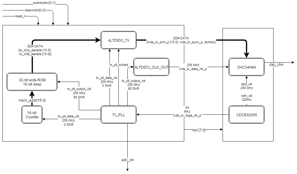
The function is as described below. The CDCE62005 generates a clock used to generate all other clocks on the TSW1400. A clock signal is send to a 16-bit counter, the output of which feeds to the address input of ROM. The ROM contains the signal to be created with the DAC, and is clocked 90 degrees off of the counter. The ROM is 32-bits wide, so each word contains both the channel A and channel B signals. This is fed to ALTDIDO_TX which is clocked -90 degrees out of phase of the memory. ALTDIDO_TX combines the two 16-bit SDR data streams into a single DDR 16-bit data stream..

TX_PLL is fed into ALTDIDO_CLK_OUT which create the clock corresponding to the DAC data. 

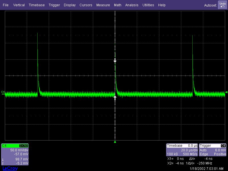
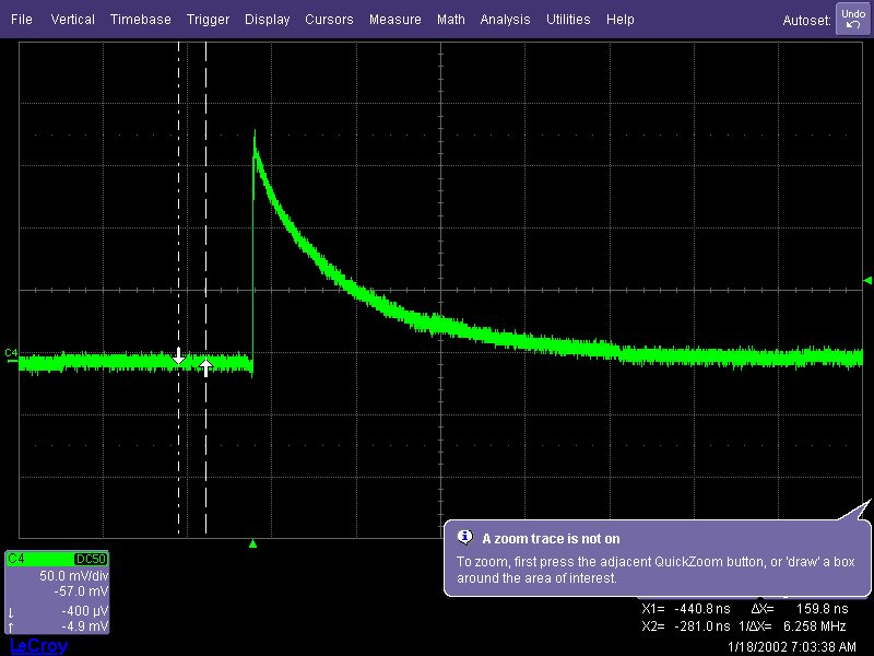
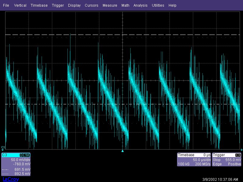
With this setup, I am getting a lot of systematic 'noise' from the DAC, similar to my problems previously, and there is huge distortion on the signal. Here is an example of a ramp signal sent to the DAC:

  • Nicholai,

    Please describe your expected waveform and the problem area. Are you expecting a nice stair case ramp from the DAC output from start to finish without any deadtime? Have you also configured the DAC output to resistor terminated to avoid a high pass filter effect?

    The ramp almost looks like a step response. Is the duration of the step response matching each sample transition and the overall sample duration? (i.e. 2^16 * sample duration).

    Also, what is the bandwidth of your scope + probe? Most of the signal distortion is caused by the signal being bandwidth limited by the measurement equipment. Please also note that in order to remove some of the transients due to the sample and hold circuit, an anti-aliasing low pass filter is needed. The DAC's output is similar to a stair-case step due to the sample and hold circuit, and will cause the output waveform not being smooth. You will need to refer to the following app note for detail:

    http://www.ti.com/lit/an/slaa523a/slaa523a.pdf

    You mentioned that you are using the TSW1400. Is the result the same when you load the same pattern into the TSW1400 using the default HSDC PRO firmware?

    I cannot troubleshoot your FPGA firmware and can only help with your DAC setup. I suggest that you make sure the DAC is configured correctly using the HSDC PRO firmware and software before moving to your own firmware development. You may attached your DAC setup configuration and let me know your expected output waveform. I can help you verify from the DAC setup perspective.

    For all firmware development, you will have to consult with Altera support.

    -Kang

  • Thank you much for your reply, Kang.

    Please describe your expected waveform and the problem area. Are you expecting a nice stair case ramp from the DAC output from start to finish without any deadtime? Have you also configured the DAC output to resistor terminated to avoid a high pass filter effect?

    Yes, I am expecting a nice stair case ramp from start to finish, without deadtime. As soon as the ramp goes to zero, the next period should start and the signal goes back to the maximum. I have not configured the DAC to avoid the HPF effect. Can you point me to instructions on how to do this? This might very well be part of the issue.

    The ramp almost looks like a step response. Is the duration of the step response matching each sample transition and the overall sample duration? 

    Yes, I have the signal 2^16 samples long, increasing by one every time.

    Also, what is the bandwidth of your scope + probe? Most of the signal distortion is caused by the signal being bandwidth limited by the measurement equipment. Please also note that in order to remove some of the transients due to the sample and hold circuit, an anti-aliasing low pass filter is needed. The DAC's output is similar to a stair-case step due to the sample and hold circuit, and will cause the output waveform not being smooth. You will need to refer to the following app note for detail:

    The scope is a 5 GS/s with 1 GHz backend, the cable is a high frequency cable (multi GHz)

    You mentioned that you are using the TSW1400. Is the result the same when you load the same pattern into the TSW1400 using the default HSDC PRO firmware?

    Yes. Here is the HSDC Pro Experiment Results:


    You may attached your DAC setup configuration and let me know your expected output waveform. I can help you verify from the DAC setup perspective.

    I have attached the DAC configuration file.

    dac_config_8_14_15.txt
       x00	   x0004
       x01	   x0100
       x02	   x0000
       x03	   xF000
       x04	   xE7BB
       x05	   x0260
       x06	   x3B00
       x07	   x0000
       x08	   x0000
       x09	   x8000
       x0A	   x0000
       x0B	   x0000
       x0C	   x0000
       x0D	   x0000
       x0E	   x0000
       x0F	   x0000
       x10	   x0000
       x11	   x0000
       x12	   x0000
       x13	   x0000
       x14	   x3333
       x15	   x3333
       x16	   x3333
       x17	   x3333
       x18	   x2067
       x19	   x0834
       x1A	   x6820
       x1B	   x0000
       x1C	   x0007
       x1D	   x0054
       x1E	   x0000
       x1F	   x8882
       x20	   x8800
       x22	   x1B1B
       x23	   x0000
       x24	   x0000
       x25	   x0000
       x26	   x0000
       x27	   x0000
       x28	   x0000
       x29	   x0000
       x2A	   x0000
       x2B	   x0000
       x2C	   x0000
       x2D	   x0000
       x2E	   x0000
       x2F	   x0000
       x30	   x0000
       x7F	   x0001
    CDCE62005 Registers
    Freq:0.000000MHz
    Address	Data
    00		68400300
    01		81140321
    02		81820302
    03		EB0A0303
    04		EB0A0304
    05		00001A85
    06		04CE03B6
    07		1588BAB7
    08		20001808

    Thank you for your time, Kang.

  • Kang,

    If I wanted to remove the high pass filter effect, could I simply follow the same steps outlined here?

    e2e.ti.com/.../224608

    I would still like to measure my signal using a 50 ohm single ended scope, I just would like to remove the filtering.
  • Are there any updates to this issue?

    Thank you,
    Nicholai
  • Nicholai,

    Yes, this is a start. I also recommend you read the following app note so you understand the reason for the resistor termination.
    www.ti.com/.../slua647

    I recommend installing 50ohm near the DAC leg and use the scope's 50ohm to ground for best source/load termination.

    -Kang
  • Nicolai,

    A couple of comments on your config file after reviewing it:

    1. The CDCE62005 is programmed to output 768MHz of clock with default /1 divider (the PLL loop is configured as 19.2MHz input clock, with PLL multiplier set at 40, which is 768MHz). The DACCLK is set at /24 of 768MHz, or 32MHz clock. The FPGA clock is set at /12 of 768MHz, or 64MHz. This is fine since your DAC is set at 1x interpolation with Fdata = Fdac = 32MSPS. The 64MHz clock going into the FPGA is needed to provide the effect LVDS toggle rate of 64MSPS, I am assuming. 

    Please see attached for my suggested config. I mainly enabled the FIFO of the DAC and some minor tweaks. Please take a look. Please also refer to the following app note for detail:

    2. Since the DAC is sampling at 32MHz, or ~32ns period. Each sample transition is expected to be 32ns. With ramp of 2^16 samples or 65535 samples, the total transition is 2ms. I do not believe your scope shot shows the whole transition. I believe the step is only showing the major code transition. With the BPF response, these major code transition will show up more apparent. Please try either sine wave (if default output is used) or resistor termination to remove the BPF effect for the ramp. 

    dac_config_8_14_15_reviewed.txt
       x00	   x0084
       x01	   x0000
       x02	   x0000
       x03	   xF000
       x04	   xE7BB
       x05	   x0260
       x06	   x3B00
       x07	   x0000
       x08	   x0000
       x09	   x8000
       x0A	   x0000
       x0B	   x0000
       x0C	   x0000
       x0D	   x0000
       x0E	   x0000
       x0F	   x0000
       x10	   x0000
       x11	   x0000
       x12	   x0000
       x13	   x0000
       x14	   x3333
       x15	   x3333
       x16	   x3333
       x17	   x3333
       x18	   x2067
       x19	   x0834
       x1A	   x6820
       x1B	   x0000
       x1C	   x0007
       x1D	   x0054
       x1E	   x0000
       x1F	   x8882
       x20	   x8801
       x22	   x1B1B
       x23	   x0000
       x24	   x0000
       x25	   x0000
       x26	   x0000
       x27	   x0000
       x28	   x0000
       x29	   x0000
       x2A	   x0000
       x2B	   x0000
       x2C	   x0000
       x2D	   x0000
       x2E	   x0000
       x2F	   x0000
       x30	   x0000
       x7F	   x0001
    CDCE62005 Registers
    Freq:0.000000MHz
    Address	Data
    00		68400300
    01		81140321
    02		81820302
    03		EB0A0303
    04		EB0A0304
    05		00001A85
    06		04CE03B6
    07		1588BAB7
    08		20001808

  • Looking at channel D as a model, should I not be removing T1? Or am I just installing both R16 and R13 to short out the inductor, and installing a 50 ohm somewhere else? I am unsure of your instructions.
  • Nicholai,

    Let's try the following for channel D:
    1. assuming default schematic, remove R110 and R111
    2. change R37 and R39 to 25ohm.
    3. use scope probe in High Z mode, probe directly at R37 and R39. This is now in resistive termination setup.

    -Kang
  • Kang,

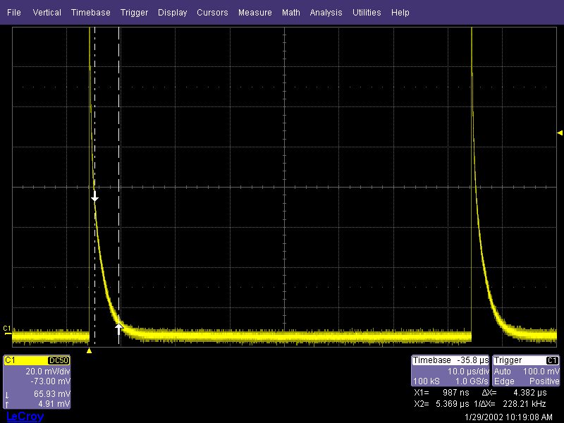
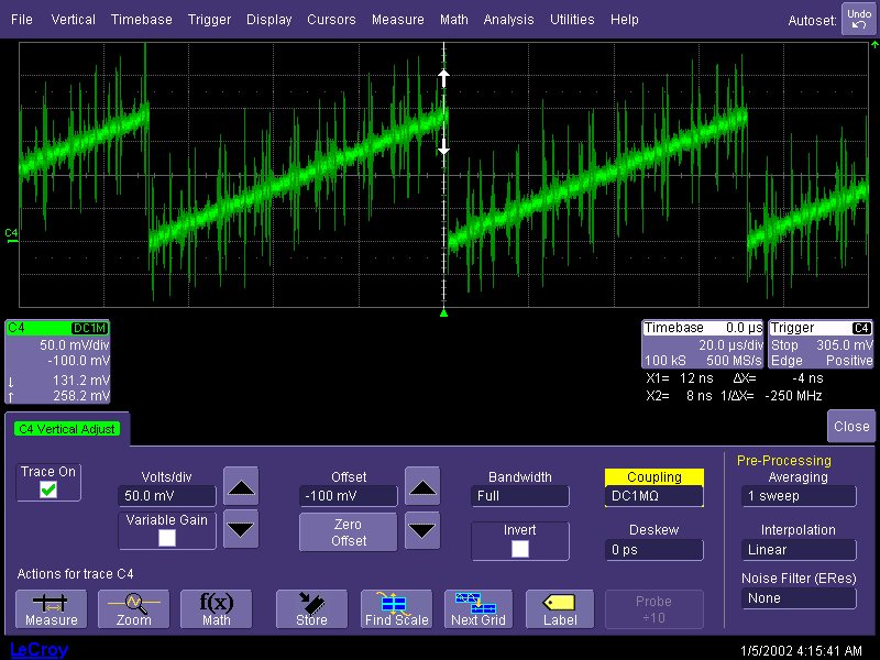
    Thank you for your work on this. I have made the modifications you suggested and ran the experiment (resistor termination). The results look significantly better. Here is the output of the DAC:

    As we can see, the DAC output is significantly closer to what we expected to see. There is a huge amount of noise still. Do you think this is simply because I am not currently using any anti-aliasing LPF for this measurement? Usually I'd expect more distortion, this looks like high frequency noise to me. What do you think?

    My second question is- if I wanted to make the resistor terminated output at the SMA, is there a suggested way to go about this? I can:

    1. Remove T11, bridge 3-4 of T11 and 1-6 of T11 (or install large 0 Ohm resistors)
    2. Remove T4
    3. Install R36, R40, and R42

  • Nicholai,

    This looks like error glitch from your FPGA timing error. I recommend that you measure the setup/hold on your FPGA output and close the timing. At such low data rate, setup/hold timing requirement should be easy to meet. The DAC itself does not generate these type of glitches.

    You configuration for resistor termination at SMA is correct.

    -Kang
  • Thank you Kang, I will look at the timing.

    Is there a simple way to make this single ended? Will I be able to simply measure only on A2, and accept that I am losing half of my power?
  • Kang,  

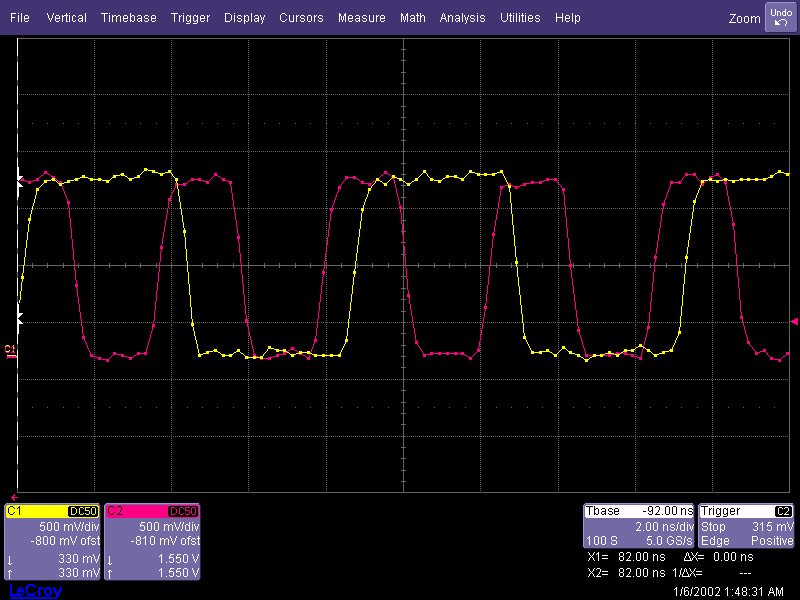
    I am trying to figure out the timing issues. Please take a look at the below figure:

    Here, the red trace is the clock, and the yellow trace is the LSB of the data, so the transitions are easily seen. While it seems like it is very close to satisfying the setup and hold, the only part I think might be an issue is the falling data and rising clock transition. However, I did try changing the input LVDS delay on DAC controller, and that didn't seem to solve the problem. Does this still look like timing to you, or perhaps something else is going on?

  • Kang,

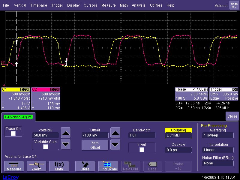
    I think I have fixed any potential clock issues I was having, but am still getting a noisy output. Here is the clock and LSB of my data, showing I am pretty well aligned (red is clock, yellow is LSB:

    The output is still bad:

    I have tried adjusting Config36 on the DAC to see if I tweaking the setup and hold times would make a difference. I tried (2,0), (5,0), and (7,0), in addition to the (0,0) it was initially set to, and this does not solve the messy output. Do you have any advice on how to move forward?

  • Nicolai,

    I suspect that these are the DAC output code transition points, and these transition voltages becomes larger due to the parasitic of the cable connections/solder joints. For your scope setup, you may want to change from full bandwidth to some sort of low pass filter. The low pass filter bandwidth is typically the Nyquist BW or Fs/2. These filters are typically used to suppress higher order images of the DAC output, which shows up on the time domain as high frequency noises.

    Take a look at the following app note to see why you need additional filters. Also, check your solder/cable connections as parasitic L/C causes ringing to these transitions.
    www.ti.com/.../slaa523a.pdf