This thread has been locked.

If you have a related question, please click the "Ask a related question" button in the top right corner. The newly created question will be automatically linked to this question.

ADS1247: Problem with getting the Ref voltage output

Part Number: ADS1247

Hi,

I am trying to use an ADS1247 to measure small voltage generated by a thermocouple sensor. I have setup the device such that I initialize it by doing a RESET (0x06) followed by 0x40 to write setup and then a constant conversion to see the output. I have sent the following

WriteSPI(0x40); //Write CMD 
WriteSPI(0x03); //Number of register to write 4 so 4-1, 3 to be sent as per datasheet
WriteSPI(0x01); //MUX Control Register AN0 POS and AN1 NEG
WriteSPI(0x00); //BIAS No BIAS set
WriteSPI(0x35); //MULTIPLEXER Control: Internal Oscillator, Internal Ref ON during Conversion, Internal Ref selected, Monitor Control REF0
WriteSPI(0x00); //Control PGA=1 DR =5SPS

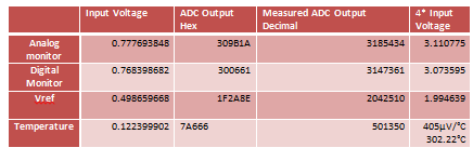
When looking at the output I was expecting the 1/4 of Vref which should be 512mV or on the reading from the ADC a value near 0x200000 however I am not getting such value but 0x7FFFFF. Below is the schematic of the hardware used

Thank you for your help

  • Fabien,


    I don't see anything wrong in the code snippet that you've sent. It looks correct for what you've describe what you want to do.

    For the schematic, the VREFCOM should be connected to ground. The schematic currently shows it floating. The VREFCOM requires a connection to an AC ground node through a resistance of less than 10Ω. Without that, the reference may not be stable.

    If you do have the VREFCOM connected to ground and the reference hasn't turned on, check to see that the reference has turned on after the command. I would also check that /RESET and START are both high and that the SPI communications are getting through by writing to and reading from the registers.

    At this point, I would guess that VREFCOM connection is the problem. However, if it doesn't pan out, post back and we can check the other suggestions.


    Joseph Wu
  • Thanks for the quick reply. I will check this first thing in the morning.
  • I have fixed the problem and I am now reading the following on the ADC:


    It is not the 2.048V I was expecting but close. The output voltage on the pin is 1.8V (Bit low)

  • I have done more test.

    Using a 3.2V PSU to power the ADC, and with register 0x02 set as 0x30 and 0x03 as 0x00 I obtained the following:

    Since the above where not optimum but acceptable to do further test, I tried to put another PSU as an input using a voltage divider. Two input circuit were tested with the following results:

    I then decided on test 2 to remove PSU and short the input but did not get the expected 0V. Can you advise on those results?

    Thank you

  • Fabien,


    Are you routing the internal reference to REF0 and then using the system monitor to read the reference? If that is the case, then I wouldn't be surprised that the measurement is a few percent off. The system monitor was designed to be a coarse measurement, using a resistor divider to measure REFP0 against the internal reference. The idea was to make a quick measurement to see if the external reference was still available when making a ratiometric measurement with an RTD. A measurement of just over 2V is probably good.

    However, you mention that the output voltage on the pin is 1.8V. That concerns me. This should be very close to the 2.048V reference value. A bad value like that would lead me to think that you either have a large load on the reference, or that you might be oscillating. On top of a low impedance connection to an AC ground, you also must have the capacitance to keep the reference stable.

    I'd look over the reference connections and make sure the value is correct.


    Joseph Wu
  • Fabien,


    I just noticed your new post. Just looking at the test schematics, the big problem that I see is that AGND isn't a valid input. The PGA has an input range because it is set up like an instrumentation amplifier. At the least restrictive input range with PGA=1, the analog inputs are valid from AVSS+0.1V to AVDD-0.1V, in your setup, that would be from 0.1V to 4.9V.

    The problem is the PGA output. The PGA isn't capable of driving the output all the way to ground or all the way to the positive supply. Like any other amplifier, there's a limitation on the output drive. The input range is more restrictive when the PGA is in gain. If you're in high gain, you need to be near midway between ground and supply so that the input is within the PGA range.

    As a test, you could use the same voltage divider, but tie the bottom of the resistor divider to the VREFOUT pin. This would set the input near 2V which would be fine for any gain.


    Joseph Wu
  • Thanks Joseph.

    I have tried the same divider with VREFOUT on the resistor and I am getting

  • Fabien,


    I'm not sure why the numbers are so far off from expected. How do you have the device set up? What do you have written into the configuration register? Because the ADC output value is so large, the reference voltage might be much smaller than expected.

    Originally, you had an external input for VREF going into REFP0 and REFN0. Are you using an external reference or are you using the internal reference?

    Out of curiosity, was the VREFCOM unconnected as I had seen in your first post?


    Joseph Wu
  • I am using internal reference and I indeed fixed the problem with VREFCOM. The device is set up with registers
    ControlRegister (0x02) = 0x30;
    MuxCalRegister (0x03)= 0x00;
  • Hi,

    Can you help clarifying the below:

    1. Is it possible to get the ADS1247 to work on unipolar 0-3.3V with internal clock like I am trying to do?

    2. Do I need to balance the inputs like suggested in the datasheet unsing 1M pull-up, 1M pull down?

    Test conducted today with the below circuit: (with and without the 1M on the input)

    With the 1M, I obtained 0x7FFFFF when reading conversion and nothing was plugged in while when input were shorted, I obtained 0x46B4 but expected 0x3FFFFF as it would be mid-range. Same test was done without the 1M, and when input were shorted, I obtained a value constantly changing between 0x4F1 and 0xFFFF58.

    I also tried to put 1M between the inputs when having pull up and pull down and obtain 1.1V as expected. When replicating the test with 10ohms, I obtained 3.5mV instead of 16.5uV (if this makes sense). I am not sure why the device cannot work on small voltage

    I am using a pic16LF1788 to communicate with the device.

    Thanks for your help

    Fabien

  • Fabien,


    First, I would like you to read out all of the registers and report them back. I'd asked that earlier, but you only gave me two of the registers. The point is that maybe something else is set other than what you expect. I would also like you to include the calibration registers just to make sure the values close to expected. It would also be better if you read the calibration register instead of telling me what you've written, just in case there was a mistake in your setup.

    The ADS1247 should work with a unipolar 3.3V supply with an internal clock. It is a common configuration. However, I thought you were using a 5V supply. In your previous posts, they show a 5V source for the input and I had thought that you had used the same for the analog supply. I don't think this would normally be a problem, but if you accidentally over-voltaged the input pin, then you might damage the device.

    The 1M pull-up/pull-down resistors are typically used for thermocouple biasing. I don't remember that being mentioned in the datasheet, but they give thermocouples a DC operating point at mid supply. If you're not measuring a thermocouple, I'd leave these resistors out. If you have the these resistors in, and the inputs are floating, these pull-up/pull-down resistors will pull apart the inputs and give a reading of 7FFFFFh. If the resists are in, and the inputs are shorted, the input reading should basically be 0 (not including the offset and noise). If you are getting between 4F1h and FFFF58h this translates to +1265 to -168. This appears to be a lot of noise, but it depends on your data rate (I assume that your PGA is 1).

    If you're having trouble measuring the 1M/10Ω divider. I'd suggest a different measurment to start. Replace those resistors with a 1k/1k divider and make sure that value is correct. Right now you're just testing the device in a gain of 1, and you should start with larger voltages. With smaller voltages, the errors that you might see start to add up fast. Leakage and input biasing currents have a large effect in the measurement, especially if the voltages are very small.

    I'd note that the input measurements of 351Eh and 37BBh translate to about 3mV, which is something you should be able to see with a precision multimeter. Note that making measurements with the multimeter and taking measurments with the ADC at the same time may cause noisier ADC readings. The ADC works with periodic capacitive sampling which can be disrupted by the multimeter's measurements.


    Joseph Wu

  • Register read (obtained using 0x20 command)

    Register

    00

    01

    02

    03

    04

    05

    06

    07

    08

    09

    0A

    0B

    0C

    0D

    0E

    Value

    01

    00

    30

    00

    00

    00

    00

    80

    0C

    40

    90

    FF

    00

    00

    00


    I use a 3.3V supply with the last schematic shown. AVCC and AVDD are both 3.3V and last time I used an external PSU at 5V for a voltage divider purpose and have the ability to read small voltage.

    The intent is to be able to measure voltage differential and surface temperature using a thermocouple which based on the datasheet is the reason for the 1M pull up/pull down addition.


    The code used is such as:

    void main (void)

    {  

       //Init SPI

       //Reset Device

       ResetSPIDevice();

       InitialiseSPIDevice();

       SetContinuousConversion();


       while (1) {

           if (!DRDY) {

               CheckLastConvertedValue(Data);

           }

       }

    }


    void ResetSPIDevice(void)

    {

       //IReset SPI Device

       SPI_CSN = 1; // CSN high

       SPI_SCK = 0; // SCK low

       SPI_START = 0;


       IOCIE = 1; //interrupt on change for DRDY

       WaitForDRDY ();  


       SPI_CSN = 0; // CSN low

       Wait(80); //Wait 80ms

       SPI_START = 1;


       WaitForSDI = GetTimer1CounterNow();

       //Delay waiting for device to be ready

       Wait(10); //Wait 10ms

       //Reset Device

       WriteSPI(0x06); //Write CMD With Register Nbre


       Wait(10); //Wait 10ms

       SPI_START = 0;

       Wait(10); //Wait 10ms

       SPI_CSN = 1; //CSN high*/

    }


    void InitialiseSPIDevice(void)

    {

       uint8_t ReadValues[16];

       uint8_t i;//flag when reading configuration


       ResetDRDY();

       SPI_CSN = 0; // CSN low

       Wait(10); //Wait 10ms

       SPI_START = 1;

       Wait(10); //Wait 10ms


       //Configure the Device

       WriteSPI(0x40); //Write CMD With Register Nbre

       WriteSPI(0x03); //Number of register to write 4

       WriteSPI(0x01); //MUX Control Register AN0 POS and AN1 NEG

       WriteSPI(0x00); //BIAS No BIAS set

       WriteSPI(ControlRegister); //MULTIPLEXER Control Internal Oscillator, Internal Ref ON during Conversion, Internal Ref selected, Monitor Control

       WriteSPI(MuxCalRegister); //Control PGA=1 DR =1000SPS


       //Check by Reading

       WriteSPI(0x20); //Write CMD With Register Nbre

       WriteSPI(0x0E); //Write CMD With Register Nbre

       for(i=0;i<15;i++)

           ReadValues[0] = ReadSPI(0xFF);


       //Delay waiting for device to be ready

       Wait(80); //Wait 80ms


       //Send SYNC

       WriteSPI(0x04);

       WriteSPI(0x04);


       Wait(10); //Wait 10ms


       SPI_START = 0;


       Wait(60); //Wait 10ms

       SPI_CSN = 1; // CSN high

       Wait(80); //Wait 80ms

    }


    /** @brief SetContinuousConversion */

    void SetContinuousConversion(void)

    {

       SPI_CSN = 0; // CSN low

       Wait(10); //Wait 10ms

       SPI_START = 1;

       Wait(10); //Wait 10ms

       //Send Enable constant conversion

       WriteSPI(0x14); //Write CMD With Register Nbre

       Wait(10); //Wait 10ms


    }


    /** @brief CheckLastConvertedValue */

    void CheckLastConvertedValue(uint8_t *dataStorage)

    {


       SPI_CSN = 0; // CSN low

       Wait(10); //Wait 10ms

       WriteSPI(0x12); //Write CMD With Register Nbre

       dataStorage[2] = ReadSPI(0xFF);

       dataStorage[1] = ReadSPI(0xFF);

       dataStorage[0] = ReadSPI(0xFF);  

       Wait(10); //Wait 10ms

       //CS LOW, START High

       SPI_CSN = 1; // CSN high

    }

  • I also done the test with the 1K resistors as mentioned above and got the following ( 3 x 1K with the positive and negative inputs used to measure the voltage drop across the middle resistor and  analogue supply (3.16V used)

    Experiment

    With an analog supply of 3.16V, and a gain of 1 using the above setup, the value expected was 1.05V

    Samples read in 0.2s intervals (5SPS)

    HEX

    Dec

    Voltage

    Difference with Expected

    004111B8

    4264376

    1.041107422

    0.008892578

    0040EF01

    4255489

    1.038937744

    0.011062256

    0040CAE6

    4246246

    1.036681152

    0.013318848

    0040D7D3

    4249555

    1.037489014

    0.012510986

    0040F866

    4257894

    1.039524902

    0.010475098

    0040EDC6

    4255174

    1.03886084

    0.01113916

    0040C65D

    4245085

    1.036397705

    0.013602295

    0040DD59

    4250969

    1.037834229

    0.012165771

    0040DD85

    4251013

    1.037844971

    0.012155029

    0040FBC4

    4258756

    1.039735352

    0.010264648

    0040F70A

    4257546

    1.039439941

    0.010560059

    0040D65B

    4249179

    1.037397217

    0.012602783

    0040D181

    4247937

    1.037093994

    0.012906006

    0040A3DE

    4236254

    1.034241699

    0.015758301

    0040FCF3

    4259059

    1.039809326

    0.010190674

    0040D24C

    4248140

    1.037143555

    0.012856445

    0040C510

    4244752

    1.036316406

    0.013683594

    0040D559

    4248921

    1.037334229

    0.012665771

    0040CD1D

    4246813

    1.03681958

    0.01318042

    0040BDFF

    4242943

    1.035874756

    0.014125244

    0040EDD6

    4255190

    1.038864746

    0.011135254

    0040EB22

    4254498

    1.038695801

    0.011304199

    0040E0E7

    4251879

    1.038056396

    0.011943604

    0040F1AB

    4256171

    1.039104248

    0.010895752

    0041160D

    4265485

    1.041378174

    0.008621826

  • Fabien,


    I've looked over your register configuration and everything looks correct. I had been concerned that there was some error in the configuration with the calibration, and I wanted to verify the settings for the rest of the device. However, I didn't see anything out of place.

    With your last post, these are the settings:

    Register values (in order from 00h)
    01 AIN0/AIN1 inputs
    00 No bias voltages used
    30 internal oscillator, int ref on, int ref selected, normal operation
    00 PGA=1, 5SPS
    00 OFC1
    00 OFC2
    00 OFC3
    80 FSC
    0C FSC
    40 FSC
    90 ID registers, DOUT=DOUT, IDAC off
    FF IDACs disconnected
    00 GPIO disabled
    00 GPIO output
    00 GPIO low

    I looked through the code, but didn't see anything unusual. However, I don't do a lot of coding, so I'm not the most qualified to find problems. Looking at your data, It looks rather noisy to me. You have swings of several millivolts and with the digital filtering in the device, I would have guessed that you would have much smaller noise in your measurement.

    I used a setup to duplicate your results. I have a set of three 1kΩ resistors to set up a divider, and make measurements with the center resistor. I set up the ADC in the same way you do. I enable the internal reference and use the internal reference as the ADC reference. The ADC is set to PGA=1, at 5SPS.

    Then I verify the reference. Checking it, I get 2.048335V at VREFOUT checking it with an Agilent 3458A.

    The supply I use is an Agilent E3631A power supply, with a 6V range. Then I set the output to 3.3V. With 100 output data, I get an average output code of 4502385, which translates to about 1.099215V. The standard deviation of the output code is 111 codes which is significantly smaller than your noise. This is about 27uV. I ran the supply up to 5V, and got an average output code of 6823401 (1.665869V) and the standard deviation rose to 129 codes (32uV).

    Just to check, I replaced the supply with a low noise Data Precision 8200. This is basically a large DAC, with low noise and setting resolution down to 10uV. Starting on the 3.3V as an output, I got an average output code of 4504785 (1.099806V) and the standard deviation was very small at 6.64 codes (1.6uV). Going to the 5V output, I got an average output code of 6825637 (1.666416V) and the standard deviation rose to 8.0 codes (1.95uV). I'll attach the excel file for you to look at it.

    If you're problem is noise, I'd make sure that the supplies don't have much ripple or glitching on them. Additionally, I'd make sure the source that you are measuring and the reference are also low noise. If you use the internal reference, I wouldn't load it with anything.

    Also, If you are having problems with measurements using smaller input voltages, I'd start with small steps. I did have a change to take the three 1kΩ resistors, and replace the center, measured resistor with a 1Ω resistor. Then I ramped the voltage from 1V to 5V in 1V steps. The result was a value of 500uV steps from 500uV to 2.5mV. Again, the standard deviaion in noise was 1.5uV or less.


    Joseph Wu
  • Fabien,

    I'd forgotten the attachment....

    Joseph Wu

    Test1.xlsx

  • Thanks for the feedback.

    If I do internal checks like Vref/4 using the 0x3D settings in register 0x02 and have value not as stable as you. What would be the source of the problem?

    When I checked that register today, the value returned as not as stable as the one you obtained.

    Fabien

  • Hi Fabien,

    Joseph is out of the office today, so I will pick up where he left off. Joseph did a direct voltage measurement of the VREFOUT of the ADS1247. You are making a measurement when using the system monitor of an external reference. As we know nothing about how this reference is established (sourced) or how it is connected it is quite possible this external reference is very noisy.

    The spreadsheet Joseph attached to his post showed specific voltage sources and conditions. Quoting Joseph "If you're problem is noise, I'd make sure that the supplies don't have much ripple or glitching on them. Additionally, I'd make sure the source that you are measuring and the reference are also low noise. If you use the internal reference, I wouldn't load it with anything."

    I would suggest you probe your voltage sources with an oscilloscope to determine the level of noise (please send pictures of these scope shots). Also, pictures of your setup may also help in understanding what you are doing and what may be causing noise.

    Best regards,
    Bob B
  • Hi,

    I have checked my supply and had to add capacitor on both analog and digital supply. My Vref is now more stable and is as shown below:

    HEX Dec Voltage Value x 4
    001FA86C 2074732 0.506526 2.026105
    001FA869 2074729 0.506526 2.026103
    001FA862 2074722 0.506524 2.026096
    001FA85B 2074715 0.506522 2.026089
    001FA876 2074742 0.506529 2.026115
    001FA866 2074726 0.506525 2.0261
    001FA86D 2074733 0.506527 2.026106
    001FA85F 2074719 0.506523 2.026093
    001FA866 2074726 0.506525 2.0261
    001FA868 2074728 0.506525 2.026102
    001FA873 2074739 0.506528 2.026112
    001FA868 2074728 0.506525 2.026102
    001FA86E 2074734 0.506527 2.026107
    001FA86A 2074730 0.506526 2.026104
    001FA865 2074725 0.506525 2.026099
    001FA85F 2074719 0.506523 2.026093
    001FA867 2074727 0.506525 2.026101
    001FA855 2074709 0.506521 2.026083
    001FA85E 2074718 0.506523 2.026092
    001FA860 2074720 0.506523 2.026094
    001FA86E 2074734 0.506527 2.026107
    001FA860 2074720 0.506523 2.026094
    001FA85B 2074715 0.506522 2.026089
    001FA852 2074706 0.50652 2.02608
    001FA85D 2074717 0.506523 2.026091
    001FA854 2074708 0.506521 2.026082
    001FA852 2074706 0.50652 2.02608
    001FA84E 2074702 0.506519 2.026076
    001FA85C 2074716 0.506522 2.02609
    001FA85A 2074714 0.506522 2.026088
    001FA85B 2074715 0.506522 2.026089
    001FA85B 2074715 0.506522 2.026089
    001FA84E 2074702 0.506519 2.026076
    001FA854 2074708 0.506521 2.026082
    001FA84E 2074702 0.506519 2.026076
    001FA855 2074709 0.506521 2.026083
    001FA854 2074708 0.506521 2.026082
    001FA85B 2074715 0.506522 2.026089
    001FA85A 2074714 0.506522 2.026088
    001FA84F 2074703 0.506519 2.026077
    001FA858 2074712 0.506521 2.026086
    001FA853 2074707 0.50652 2.026081

     I was however expecting value nearer to 2.048V. Is that going to cause problem when measuring thermocouple.

    Also I am supplying the device using 2x alkaline battery on which I see ripple oscillating within 200uV. This surely would affect my reading when looking at >10uV.

  • Fabien,


    I'm glad that your reference is now more stable. It looks like the measurement for Vref has a standard deviation of about 10uV. I will say that the internal reference voltage has min/max specification of ±10mV, and you're off by about 2mV. It's not great, but for better accuracy, you'll need to get a better reference, or do some calibration with this reference. Any reference error appears as a gain error in the ADC measurement.

    However, I'm not sure you're accurately measuring the reference. If you're using the system monitor to measure the reference, I think you're only measuring the internal reference voltage against itself, so you may only be measuring the voltage divider. If you want to know what the reference voltage is, use an external precision multimeter to measure VREFOUT. The Vref/4 system monitor was really designed as coarse check to verify the system is working (like burnout detection for RTD measurements).

    I had one last comment on your previous post. If you are using alkaline batteries for your supply, there shouldn't be any ripple unless you have a DC-DC converter on your board. Batteries should be about as clean of a supply source as possible. If you do have some ripple, I'd check for some pickup from EMI/RFI source.


    Joseph Wu