Other Parts Discussed in Thread: DLPC3435
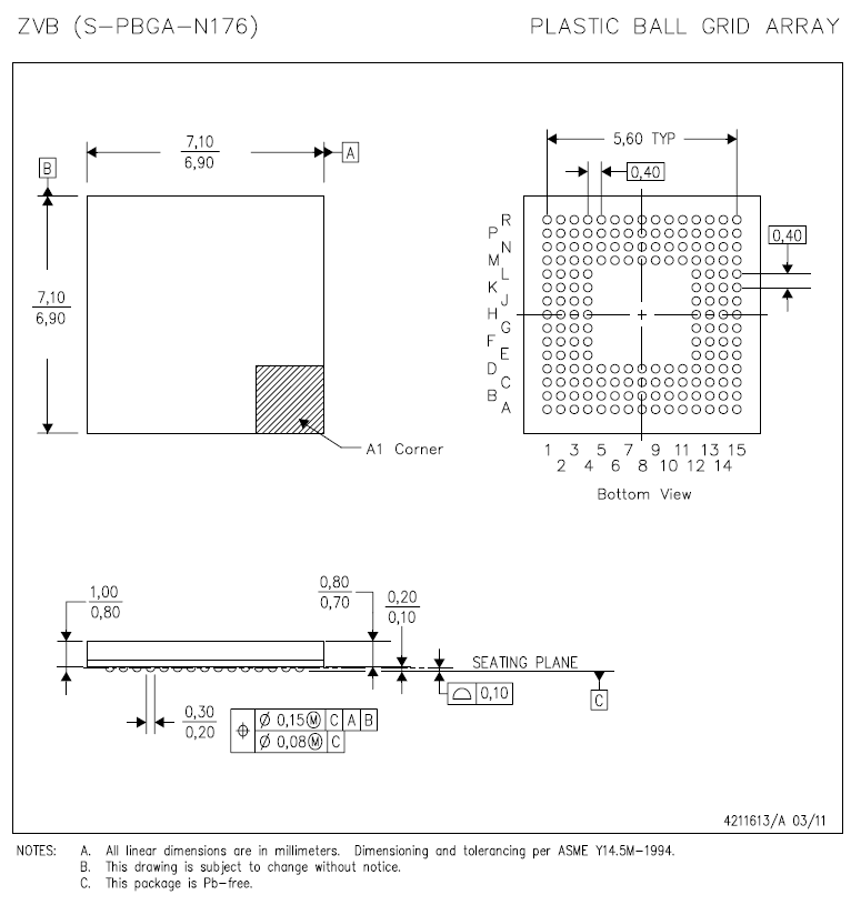
I'm currently using the dlps038c.pdf (attached) and I don't see an explicit land pattern for this package in the documentation. On page 60 there is a drawing that shows the layout of the PBGA, but there are no details about what land or stencil pattern use when designing a PCB for this chipset.