Other Parts Discussed in Thread: CDCE62005
Hello!
I made my own board based on TMDSEVM6657.
My board is not exactly same but basically almost same with TMDSEVM6657..
I got a problem between DSP and CDCE62005.
The pin map between them is like below.
CDCD62005 DSP
CH0 -> SRIOSGMIICLK : 250MHz
CH1 -> Not used
CH2 -> DDRCLK: 66Mhz
CH3 -> CORECLK: 100MHz
CH4 -> Not used
I add a port to communicate directly to the CDCE62005 through SPI pin.
This port is only used for programing the CDCE62005.
Normally the SPI pin from CDCE62005 is connected to FPGA.
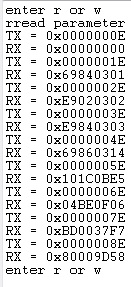
The configuration of CDCE62005 is like below.
This value was copied from the EVM FPGA code.
0: 0xE9840320
1: 0x69840301
2: 0xE9020302
3: 0xE9840303
4: 0x69860314
5: 0x101C0BE5
6: 0x04BE0F06
7: 0xFD0037F7
After the board has been booted up using with EVM FPGA code , I could see a sinewave coming only from ch2, ch3 of CDCE62005.
In case of ch0, I could also see sinewave from it but it was for very short time.
This FPGA code is not exactly same with the EVM's.
A part of the code is attached as a name of "modificaiton.zip".
And If I use my FPGA code, I can see sinewave from all of ch0 , ch2 and ch3.
This code is different than the "modificaiton.zip".
Could you please look over the attached file of "my_code.zip".
This code is very simple and just make a connection between external port and CDCE62005 SPI pin.
Using with this code, I can access to the register of CDCE62005 through SPI.
From the register, I have confirmed that the PLL was locked.
If I ask you again, what kind of condition makes the output of CDCE62005 off.
Regards
Yun-Seok Cho