This thread has been locked.

If you have a related question, please click the "Ask a related question" button in the top right corner. The newly created question will be automatically linked to this question.

Troubles in connecting to OMAP-L138

Other Parts Discussed in Thread: OMAP-L138, OMAPL138

I made my own board based on OMAP-L138.

The version of my CCS is CCSv4.1.2.

And my JTAG emulator is SEED-XDS560PLUS.

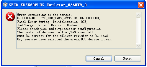
When it connects to OMAP-L138’s  ARM9 core,the following error would occur :

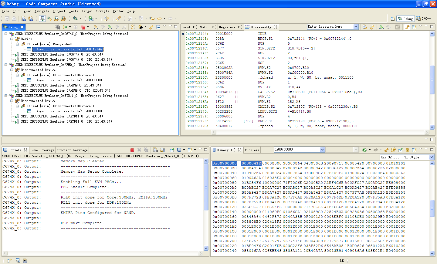
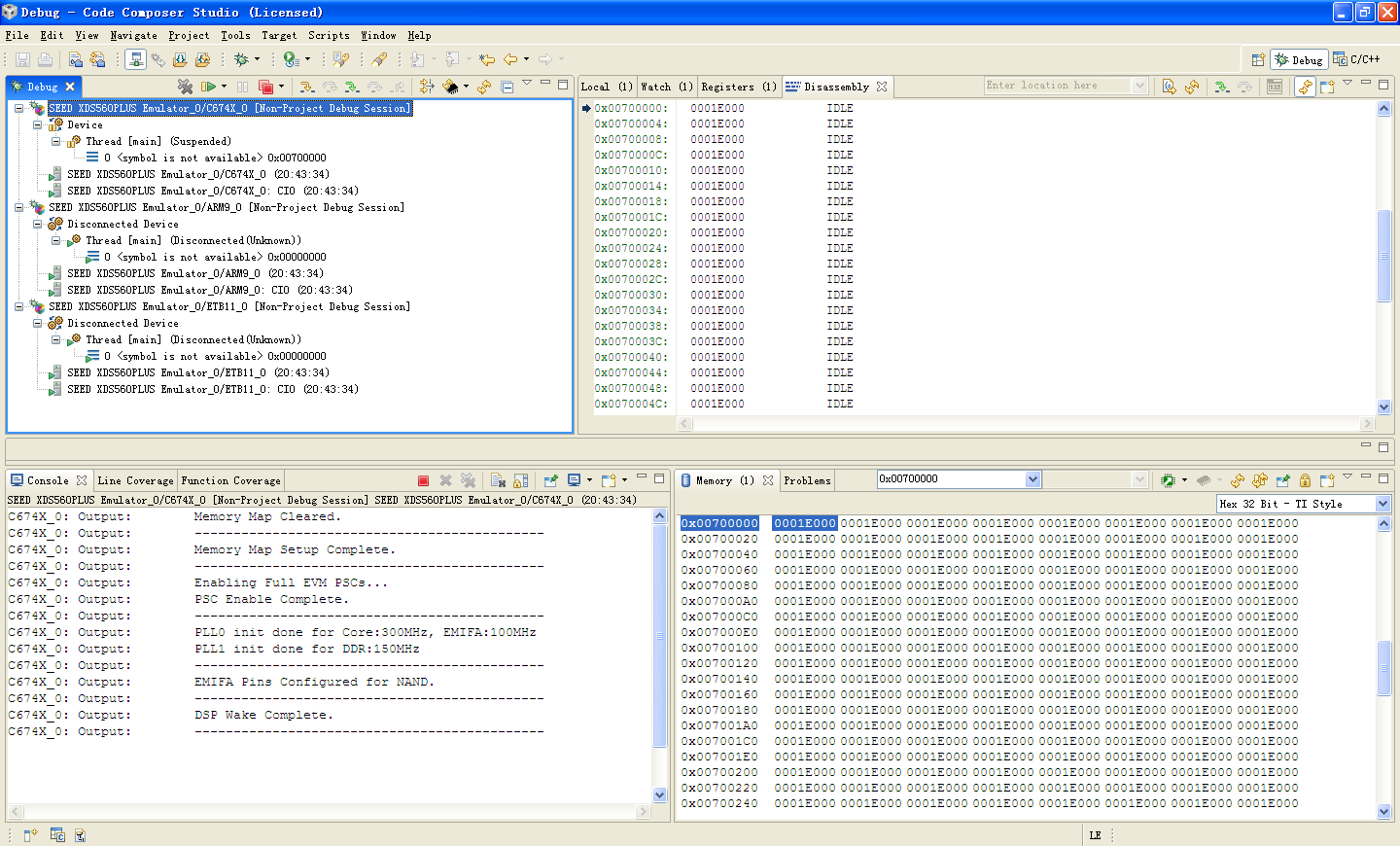
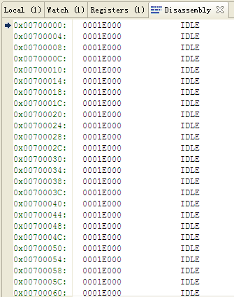
And it could connect to OMAP-L138’s C674x core ,but the codes in DSP L2 ROM are all IDLEs,which means there's no fixed bootloader codes in it :

The power and clock and reset signals are correct. And my CCS and emulator work well with other OMAP-L138 boards.

So does my OMAP-L138 chip get damaged? Could anyone help me?

  • Hi Cicy,

    Please make sure that ou have the appropriate drivers for the SEED emulator, and also check your hardware connections.

    There are several forum posts with the same error for different emulators (search for error in the forums). Take a look and check if any of the problem identified could be what is happening to you:

    http://e2e.ti.com/support/dsp/tms320c5000_power-efficient_dsps/f/109/t/31971.aspx

    http://e2e.ti.com/support/development_tools/code_composer_studio/f/81/t/127572.aspx

    http://e2e.ti.com/support/development_tools/code_composer_studio/f/81/t/92608.aspx


  • Hi Mariana,

    Thanks a million for your response.But actually,I've already scanned such posts and almost all other similar posts several days ago.And I've tried all the suggestions mentioned in them.However,my problem still exists.

    The power and clock and reset signals are correct. And my CCS and emulator work well with another same board.

    So do you think I need to change another OMAP-L138 chip?

    Best regards,Cicy

  • Hi Cicy

    Let us use this post for further clarifications on your issue, you should not have to post the same set of responses on the other thread. The DSP ROM is not visible from ARM side at location 0x007xxx , if you want to read the DSP ROM content from ARM9, please use address location 0x117xxx in CCS memory window from ARM side (you can refer to the memory map table int he OMAPL138 datasheet to understand this concept).

    Please provide a printout from the debug gel file

    http://processors.wiki.ti.com/index.php/OMAP-L1x_Debug_Gel_Files

    Additionally as Rahul mentioned in the other thread, are you making sure that the DSP clocks are enabled via GEL file or other mechanism, as by default DSP is clocked off in OMAPL138. If you are successfully able to do that on the other board, please share the steps on how you go about doing this.

    Finally, do you have local field support for this issue, who could possibly help more efficiently if you think this is a device/board problem.

    Regards

    Mukul

  • Hi Mukul,

    Thank you so much for your reply. First, I could only connect to DSP core successfully right now. So the DSP ROM IDLEs are read from the C6748 side exactly. And some hardware tests even have been passed from the DSP core, such as DDR2,NAND Flash, UART,LCD and so on. But when it connects to the ARM core, the fatal error described in the first picture above would appear.


    Second, here’s the printout from the debug gel file:

    C674X_0: Output: Memory Map Cleared.

    C674X_0: Output: ---------------------------------------------

    C674X_0: Output: Memory Map Setup Complete.

    C674X_0: Output: ---------------------------------------------

    C674X_0: Output: Enabling Full EVM PSCs...

    C674X_0: Output: PSC Enable Complete.

    C674X_0: Output: ---------------------------------------------

    C674X_0: Output: PLL0 init done for Core:300MHz, EMIFA:100MHz

    C674X_0: Output: PLL1 init done for DDR:150MHz

    C674X_0: Output: ---------------------------------------------

    C674X_0: Output: EMIFA Pins Configured for NAND.

    C674X_0: Output: ---------------------------------------------

    C674X_0: Output: DSP Wake Complete.

    C674X_0: Output: ---------------------------------------------

    C674X_0: GEL Output:  ---------------------------------------------

    C674X_0: GEL Output: |             Device Information            |

    C674X_0: GEL Output: ---------------------------------------------

    C674X_0: GEL Output: DEV_INFO_00 = 0x0B7D102F

    C674X_0: GEL Output: DEV_INFO_01 = 0x00000000

    C674X_0: GEL Output: DEV_INFO_02 = 0x0000001E

    C674X_0: GEL Output: DEV_INFO_03 = 0x00000000

    C674X_0: GEL Output: DEV_INFO_04 = 0x00000000

    C674X_0: GEL Output: DEV_INFO_05 = 0x00000000

    C674X_0: GEL Output: DEV_INFO_06 = 0x00000000

    C674X_0: GEL Output: DEV_INFO_07-DEV_INFO_08-DEV_INFO_09-DEV_INFO_10-DEV_INFO_11-DEV_INFO_12 = 0-0-0-0-0-0

    C674X_0: GEL Output: DEV_INFO_13,DEV_INFO_14,DEV_INFO_15,DEV_INFO_16 = 0,0,0,0

    C674X_0: GEL Output: -----

    C674X_0: GEL Output: DEV_INFO_17 = 0x00030403

    C674X_0: GEL Output: DEV_INFO_18 = 0x00000000

    C674X_0: GEL Output: DEV_INFO_19 =

    C674X_0: GEL Output: 0

    C674X_0: GEL Output: 0

    C674X_0: GEL Output: 1

    C674X_0: GEL Output: 0

    C674X_0: GEL Output: 0

    C674X_0: GEL Output: 

    C674X_0: GEL Output: -----

    C674X_0: GEL Output: DEV_INFO_20 = 0x0001E000

    C674X_0: GEL Output: DEV_INFO_21 = 0x0001E000

    C674X_0: GEL Output: DEV_INFO_22 = 0x00000000

    C674X_0: GEL Output: DEV_INFO_23 = 0x00000000

    C674X_0: GEL Output: -----

    C674X_0: GEL Output: DEV_INFO_24 = 0x00000000

    C674X_0: GEL Output: DEV_INFO_25 = 0x00000000

    C674X_0: GEL Output: DEV_INFO_06 = 0x00000000

    C674X_0: GEL Output: DEV_INFO_26 = 0x00000000

    C674X_0: GEL Output:  

    C674X_0: GEL Output: ---------------------------------------------

    C674X_0: GEL Output: |               BOOTROM Info                |

    C674X_0: GEL Output: ---------------------------------------------

    C674X_0: GEL Output: ROM ID: d800k176-47-48 

    C674X_0: GEL Output: Silicon Revision UNKNOWN

    C674X_0: GEL Output: Boot pins: 30

    C674X_0: GEL Output: Boot Mode: Emulation Debug

    C674X_0: GEL Output:  ROM Status Code: 0x0000004C  Description:

    C674X_0: GEL Output: Error code not recognized

    C674X_0: GEL Output:  Program Counter (PC) = 0xC2017940

    C674X_0: GEL Output: 

    C674X_0: GEL Output: ---------------------------------------------

    C674X_0: GEL Output: |              Clock Information             |

    C674X_0: GEL Output: ---------------------------------------------

    C674X_0: GEL Output: 

    C674X_0: GEL Output: PLLs configured to utilize crystal.

    C674X_0: GEL Output: ASYNC3 = PLL0_SYSCLK2

    C674X_0: GEL Output: 

    C674X_0: GEL Output: NOTE:  All clock frequencies in following PLL sections are based

    C674X_0: GEL Output: off OSCIN = 24 MHz.  If that value does not match your hardware

    C674X_0: GEL Output: you should change the #define in the top of the gel file, save it,

    C674X_0: GEL Output: and then reload.

    C674X_0: GEL Output: 

    C674X_0: GEL Output: ---------------------------------------------

    C674X_0: GEL Output: |              PLL0 Information             |

    C674X_0: GEL Output: ---------------------------------------------

    C674X_0: GEL Output: 

    C674X_0: GEL Output: PLL0_SYSCLK1 = 300 MHz

    C674X_0: GEL Output: PLL0_SYSCLK2 = 150 MHz

    C674X_0: GEL Output: PLL0_SYSCLK3 = 100 MHz

    C674X_0: GEL Output: PLL0_SYSCLK4 = 75 MHz

    C674X_0: GEL Output: PLL0_SYSCLK5 = 100 MHz

    C674X_0: GEL Output: PLL0_SYSCLK6 = 300 MHz

    C674X_0: GEL Output: PLL0_SYSCLK7 = 50 MHz

    C674X_0: GEL Output: 

    C674X_0: GEL Output: ---------------------------------------------

    C674X_0: GEL Output: |              PLL1 Information             |

    C674X_0: GEL Output: ---------------------------------------------

    C674X_0: GEL Output: 

    C674X_0: GEL Output: PLL1_SYSCLK1 = 300 MHz

    C674X_0: GEL Output: PLL1_SYSCLK2 = 150 MHz

    C674X_0: GEL Output: PLL1_SYSCLK3 = 100 MHz

    C674X_0: GEL Output: 

    C674X_0: GEL Output: ---------------------------------------------

    C674X_0: GEL Output: |              PSC0 Information             |

    C674X_0: GEL Output: ---------------------------------------------

    C674X_0: GEL Output: 

    C674X_0: GEL Output: State Decoder:

    C674X_0: GEL Output:  0 = SwRstDisable (reset asserted, clock off)

    C674X_0: GEL Output:  1 = SyncReset (reset assered, clock on)

    C674X_0: GEL Output:  2 = Disable (reset de-asserted, clock off)

    C674X_0: GEL Output:  3 = Enable (reset de-asserted, clock on)

    C674X_0: GEL Output: >3 = Transition in progress

    C674X_0: GEL Output: 

    C674X_0: GEL Output: Module 0:  EDMA3CC (0)        STATE = 3

    C674X_0: GEL Output: Module 1:  EDMA3 TC0          STATE = 3

    C674X_0: GEL Output: Module 2:  EDMA3 TC1          STATE = 3

    C674X_0: GEL Output: Module 3:  EMIFA (BR7)        STATE = 3

    C674X_0: GEL Output: Module 4:  SPI 0              STATE = 3

    C674X_0: GEL Output: Module 5:  MMC/SD 0           STATE = 3

    C674X_0: GEL Output: Module 6:  AINTC              STATE = 3

    C674X_0: GEL Output: Module 7:  ARM RAM/ROM        STATE = 3

    C674X_0: GEL Output: Module 9:  UART 0             STATE = 3

    C674X_0: GEL Output: Module 10: SCR 0 (BR0/1/2/8)  STATE = 3

    C674X_0: GEL Output: Module 11: SCR 1 (BR4)        STATE = 3

    C674X_0: GEL Output: Module 12: SCR 2 (BR3/5/6)    STATE = 3

    C674X_0: GEL Output: Module 13: PRUSS              STATE = 0

    C674X_0: GEL Output: Module 14: ARM                STATE = 0

    C674X_0: GEL Output: Module 15: DSP                STATE = 3

    C674X_0: GEL Output: 

    C674X_0: GEL Output: ---------------------------------------------

    C674X_0: GEL Output: |              PSC1 Information             |

    C674X_0: GEL Output: ---------------------------------------------

    C674X_0: GEL Output: 

    C674X_0: GEL Output: State Decoder:

    C674X_0: GEL Output:  0 = SwRstDisable (reset asserted, clock off)

    C674X_0: GEL Output:  1 = SyncReset (reset assered, clock on)

    C674X_0: GEL Output:  2 = Disable (reset de-asserted, clock off)

    C674X_0: GEL Output:  3 = Enable (reset de-asserted, clock on)

    C674X_0: GEL Output: >3 = Transition in progress

    C674X_0: GEL Output: 

    C674X_0: GEL Output: Module 0:  EDMA3CC (1)        STATE = 3

    C674X_0: GEL Output: Module 1:  USB0 (2.0)         STATE = 3

    C674X_0: GEL Output: Module 2:  USB1 (1.1)         STATE = 3

    C674X_0: GEL Output: Module 3:  GPIO               STATE = 3

    C674X_0: GEL Output: Module 4:  UHPI               STATE = 3

    C674X_0: GEL Output: Module 5:  EMAC               STATE = 3

    C674X_0: GEL Output: Module 6:  DDR2 and SCR F3    STATE = 3

    C674X_0: GEL Output: Module 7:  MCASP0 + FIFO      STATE = 3

    C674X_0: GEL Output: Module 8:  SATA               STATE = 3

    C674X_0: GEL Output: Module 9:  VPIF               STATE = 3

    C674X_0: GEL Output: Module 10: SPI 1              STATE = 3

    C674X_0: GEL Output: Module 11: I2C 1              STATE = 3

    C674X_0: GEL Output: Module 12: UART 1             STATE = 3

    C674X_0: GEL Output: Module 13: UART 2             STATE = 3

    C674X_0: GEL Output: Module 14: MCBSP0 + FIFO      STATE = 3

    C674X_0: GEL Output: Module 15: MCBSP1 + FIFO      STATE = 3

    C674X_0: GEL Output: Module 16: LCDC               STATE = 3

    C674X_0: GEL Output: Module 17: eHRPWM (all)       STATE = 3

    C674X_0: GEL Output: Module 18: MMC/SD 1           STATE = 3

    C674X_0: GEL Output: Module 19: UPP                STATE = 3

    C674X_0: GEL Output: Module 20: eCAP (all)         STATE = 3

    C674X_0: GEL Output: Module 21: EDMA3 TC2          STATE = 3

    C674X_0: GEL Output: Module 24: SCR-F0 Br-F0       STATE = 3

    C674X_0: GEL Output: Module 25: SCR-F1 Br-F1       STATE = 3

    C674X_0: GEL Output: Module 26: SCR-F2 Br-F2       STATE = 3

    C674X_0: GEL Output: Module 27: SCR-F6 Br-F3       STATE = 3

    C674X_0: GEL Output: Module 28: SCR-F7 Br-F4       STATE = 3

    C674X_0: GEL Output: Module 29: SCR-F8 Br-F5       STATE = 3

    C674X_0: GEL Output: Module 30: Br-F7 (DDR Contr)  STATE = 3

    C674X_0: GEL Output: Module 31: L3 RAM, SCR-F4, Br-F6 STATE = 3


    Thirdly, I’ve already loaded the uboot on the other board. And my steps are:

    1、 Set the boot mode of my board as Emulation Debug Mode.

    2、 Set the target configuration correctly. Make sure select OMAPL138_ARM.gel file in “initialization script” for ARM9_0 and set JTAG TCLK Frequency as 10.368MHz limit.Then save it OMAPL138.ccxml.

    3、 Launch OMAPL138.ccxml. Right-click on “SEED XDS560PLUS Emulator_0/ARM9_0 [Non-Project Debug Session]” and select “Connect Target”.

    4、 Load program “nand-writer_ccs33.out”,then run it.

    5、 Follow the clues printed in the Console to input “armais”,and then input the “ubl-nand.bin” with right path. Waiting for UBL to be written completely.

    6、 Reload program “nand-writer_ccs33.out”,and run it again.

    7、 Follow the clues printed in the Console to input “uboot”,and then input the “u-boot.bin” with right path. Waiting for UBOOT to be written completely.

    8、 Power off the board. Set it as NAND Boot Mode. And I’ve loaded kernel and file system on it already. It runs very well.


    In order to do the hardware tests under DSP. So I chose to connect the DSP core only. And I used the same gel file “OMAPL138_ARM”.The following pictures are the results between the good board and the bad one:

    Good board: after connecting, the PC located at 0x00712144, and there are bootloader codes in the DSP ROM

    Bad board: after connecting, the PC located at 0x00700000, and there are only IDLEs in the DSP ROM


    Lastly, I’m a graduated student of Xidian University which is located in Xi’an , China. So do you know anyone here could help me?


    Regards,Cicy

  • According to debug gel printout, PSC0 Information shows ”ARM  STATE = 0”.So I guess the ARM core wasn’t woken up.

    Therefore, I loaded a dsp gel file “OMAPL138_DSP.gel” and used it to wake ARM. Then it connected to ARM9_0 successfully.


    My steps in detail:

    l       Set the boot mode of my board as Emulation Debug Mode.

    l       Set the target configuration correctly. Make sure select “OMAPL138_ARM.gel” in “initialization script” for ARM9_0 and “OMAPL138_DSP.gel” for C674x_0.Also make sure set JTAG TCLK Frequency as 10.368MHz limit.Then save it as “OMAPL138.ccxml”.

    l       Launch OMAPL138.ccxml. Connect to DSP first of all.

    l       Go to Scripts→Wake Core→Wake_ARM.

    l       Connect to ARM and there’s no error shows againO(∩_∩)O~.

    l       Load program “nand-writer_ccs33.out”,and run it to write UBOOT into NAND Flash.


    By the way, when running  program “nand-writer_ccs33.out”,Console prints “DA850/OMAP-L138 part detected. It’s a DSP  boot device”, which proved my guess above. But for the other board, it  prints “DA850/OMAP-L138 part detected. Its an ARM boot device”

    As you seen, even the same OMAP-L138 chips are different inside. Interesting and wonderful,right?


    Thank all of you who care about this post. And hope it could help you,too.


    Have a nice day.Cicy

  • I posted a new question several days ago.But no body answered it.Could you help me?

    Here's the link: http://e2e.ti.com/support/dsp/omap_applications_processors/f/42/t/208579.aspx