This thread has been locked.

If you have a related question, please click the "Ask a related question" button in the top right corner. The newly created question will be automatically linked to this question.

SN74AVC4T774: Pin states when no VCCB present

Part Number: SN74AVC4T774

Hello there,

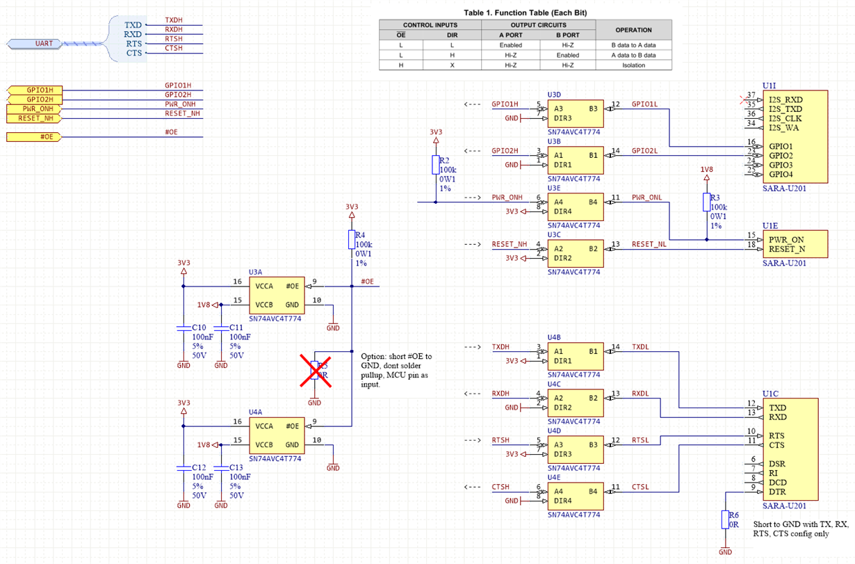
I am having a problem with an application that uses the SN74AVC4T774 chip. Here is a schematic containing this part:

The device is used for IO level shifting between main MCU (3.3 V) and GSM module (1.8 V). My question is:

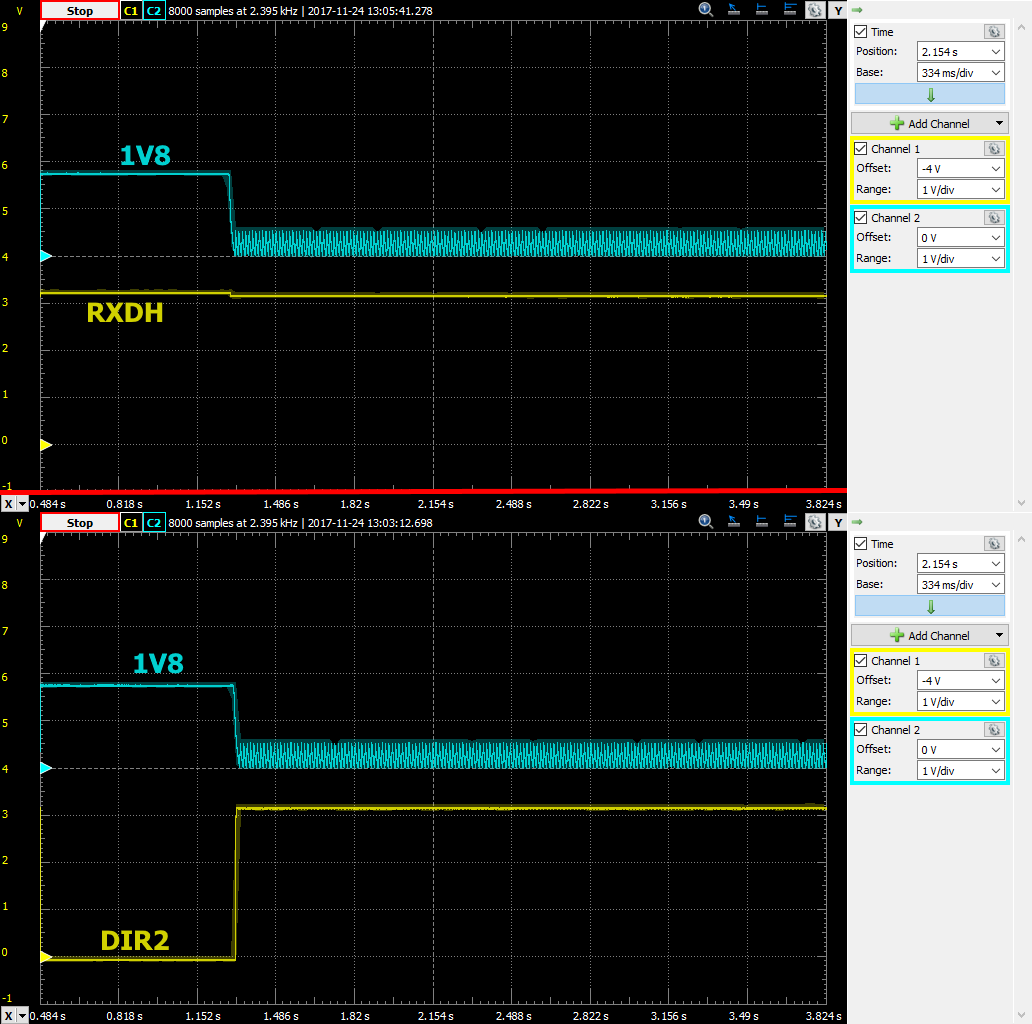
Please look at the schematic labels. What will happen to pins RXDH and CTSH (so side A outputs, side B inputs) after on part U1C the RXDL and CTSL become high impedance and the 1V8 voltage is cut-off? Because at the moment, for this situation I am getting some unspecified behavior on the RXDH line. Here is an oscillogram:

The yellow line shows the RXDH state after RXDL and 1V8 go high impedance. In case of 1.8V blackout, shouldnt the side A output pins go high impedance as well? I would appreciate all help regarding this.

  • Hi Lukasz,
    Partial power down protection (Ioff) will disable all input/output ports if one of the supply pins is brought down to 0V. That's not the same thing as being turned off, however. Sometimes a supply will still have residual voltage and the output can have unexpected behavior.

    We recommend adding a weak pull-down resistor to the Vcc pin to force the supply pin to 0V when the supply no longer can source current. This will ensure that Ioff turns on when the supply is cut off. For testing purposes, this resistor can be added in parallel with the bypass capacitor (10k to 100k should work).

    Also, even when Ioff is on, that just means the output is in a high impedance state - the voltage there will be floating at that point and could go up or down depending on many factors. If you want to ensure a certain state when the pin is in high-impedance mode, a pull-up or pull-down resistor can be added.
  • Hello, thank you for answer.

    I tried adding a pull-down to the input line one the B side, where 1V8 supply is cut-off. That did not help at all. I cannot add a pull-up, since I wont have any potential to pull it up to since 1V8 is gone.

    We recommend adding a weak pull-down resistor to the Vcc pin to force the supply pin to 0V when the supply no longer can source current. This will ensure that Ioff turns on when the supply is cut off. For testing purposes, this resistor can be added in parallel with the bypass capacitor (10k to 100k should work).

    This approach I will try out tommorow morning. But to be fair I dont think it will help.

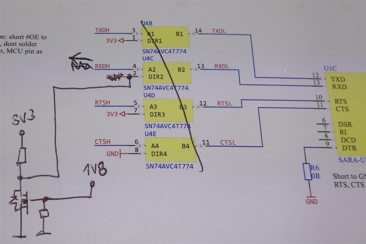
    What I am thinking of now, is to add a N mosfet transistor with very low Vgs to the design. The gate of that transistor would be driven by 1V8. The source of the transistor would be tied to GND and the drain would be tied to the DIR pins. When 1V8 is gone, the transitor would stop conducting and the DIR pins that are normally tied to GND because of the mosfet, would be pulled up by some resistor, making the A side outputs float.

    What do you think?

  • Can you get a scope shot of the 1.8V supply, RXDL, and RXDH together? That should tell us if my theory is correct or if something else is going on.
  • I only have 2 channel scope. I will try to tie the RXDH to a digital input and RXDL and 1V8 to the scope probes. Tommorow ill post the pics. Thanks.
  • Ok, here the the scope shoots. The first oscillogram shows 3 signals:

    1V8: blue

    RXDL: yellow

    RXDH: DIO0

    It seems that the 1V8 pin is not fully off like you said. It is somehow pulsing. Adding a 10k pull-down to it did not help much. Here is an another scope shoot with only 2 signals: RXDH and 1V8:

    What do you think?

  • That confirms my suspicion that the supply line is not being held at 0V -- it looks to be almost 0.7V during each cycle. Adding a resistor from 1V8 to GND should clear up the problem.
  • The second oscillogram is shoot after I added 10k pull-down to the 1V8 line. It did not help.
  • I have fixed the problem like this:

    Here are the scope shots:

    I could not figure out what is the reason for 1V8 state after GSM module shutdown. So I have introduced a workaround. As soon as 1V8 drops to around 0 - 0.7 V, the added transistor is closed, thus pulling up the DIR2 to 3V3. When DIR2 is high, the RXDH line is high-Z...